
High-quality inorganic semiconductors usually need rigid, high-temperature growth substrates, while flexible systems need a bendable final carrier. Membrane exfoliation resolves that conflict by growing first, releasing the complete device layer, and then transferring it—a process of “graft and transplant” for optoelectronics.
Semiconductor membranes Laser lift-off Flexible optoelectronics Heterogeneous integration
Obtain a high-crystalline-quality functional layer.
Chemical, laser, porous-layer, or 2D-material assistance.
Control cracks, warpage, and residual stress.
Build LEDs, detectors, and power or RF electronics.
Application background
Flexible optoelectronics are important for IoT systems, wearables, curved displays, and medical devices. Their highest-performance materials, including GaAs and GaN, are stiff and brittle and cannot normally be grown directly on a polymer film.
Three conflicts define the problem:
- Substrate compatibility: flexible polymers cannot tolerate epitaxy above 1000 °C; metals introduce lattice and thermal mismatch and contamination risks.
- Limits of organic semiconductors: organic materials bend readily but commonly have carrier mobility below 1 cm²/Vs and lower thermal and chemical stability.
- Release complexity: selective etching and laser lift-off must avoid interface damage, and large membranes are vulnerable to cracks, residual stress, and low transfer yield.
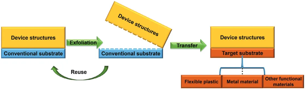
The core contradiction is simple: high crystalline quality needs a rigid growth substrate, while the application needs a flexible platform. The mainstream solution is heteroepitaxy → nondestructive release → flexible integration.
Chemical exfoliation
Chemical exfoliation selectively removes a sacrificial layer between the functional film and rigid substrate.
Process sequence
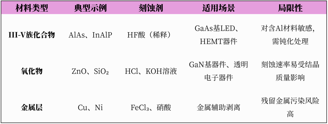
- Deposit or grow a sacrificial layer such as AlAs, ZnO, or SiO₂ on sapphire, silicon, or another rigid wafer.
- Grow GaN, GaAs, or another functional semiconductor by MOCVD, MBE, or a related epitaxial process.
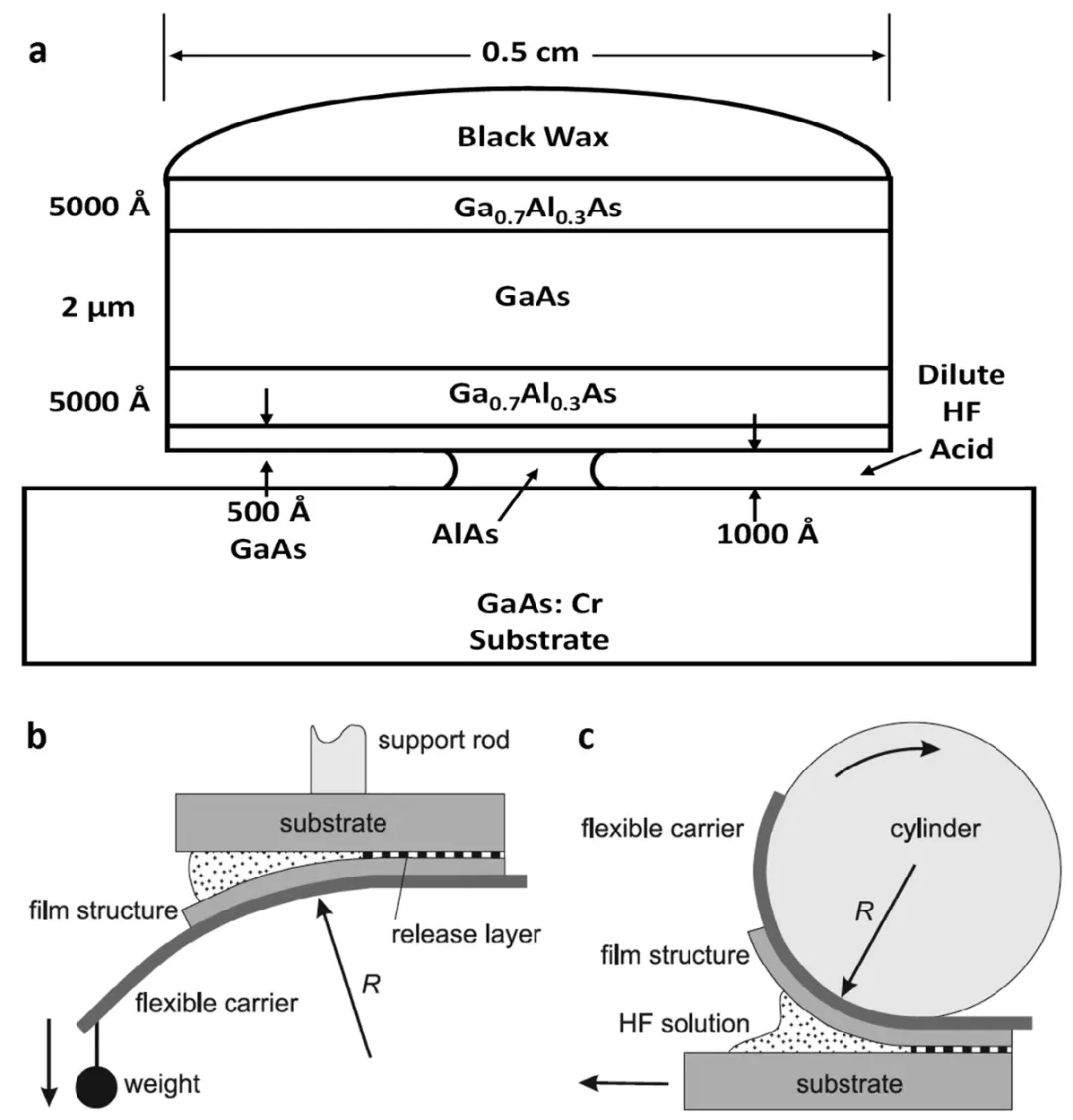
- Immerse the stack in a selective etchant such as HF or KOH to dissolve the sacrificial layer.
- Transfer the released membrane with a PDMS stamp, roller, or another carrier to PET, polyimide, or a different target.
Etch kinetics and interface control
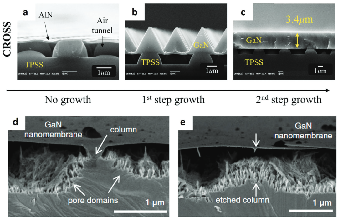
The sacrificial layer must etch much faster than the device layer, commonly with a selectivity above 100:1. AlAs can etch roughly 1000 times faster than GaAs in HF. Once the interface is removed, residual strain from lattice and thermal mismatch must be absorbed by the flexible carrier or an intermediate support to avoid curling and fracture.
Chemical release can produce an atomically smooth interface with roughness below 0.5 nm, supports uniform release of 4–6 inch wafers, and avoids costly laser equipment. Its main limitation is material choice: the sacrificial layer must be compatible with both epitaxial growth and selective etching.
Laser lift-off
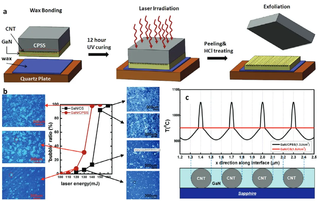
Laser lift-off (LLO) releases III–V and related films from hard substrates such as sapphire or SiC by selectively decomposing an interface layer.
Process sequence
- Grow GaN or another device structure on a transparent or optically accessible substrate.
- Irradiate through the substrate or from the device side with a wavelength absorbed strongly at the interface.
- Decompose or transform the interface and release accumulated stress.
- Transfer the separated film to polyimide, metal foil, or another target.
Laser–material interaction
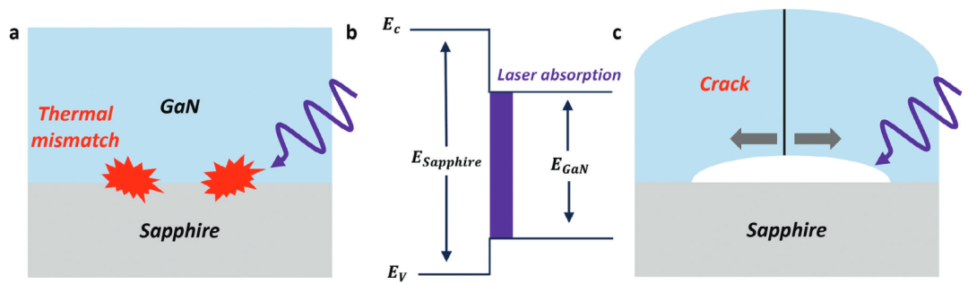
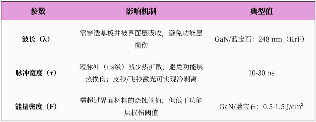
The wavelength must match the interface absorption. A common GaN/sapphire process uses a 248 nm KrF excimer laser. Its 5.0 eV photons exceed the 3.4 eV GaN band gap but remain below sapphire’s roughly 9 eV gap, so the beam passes through sapphire and is absorbed by GaN.
Rapid heating above 1000 °C decomposes the interface according to GaN → Ga + N₂↑. At high intensity, multiphoton absorption and avalanche ionization may also contribute.
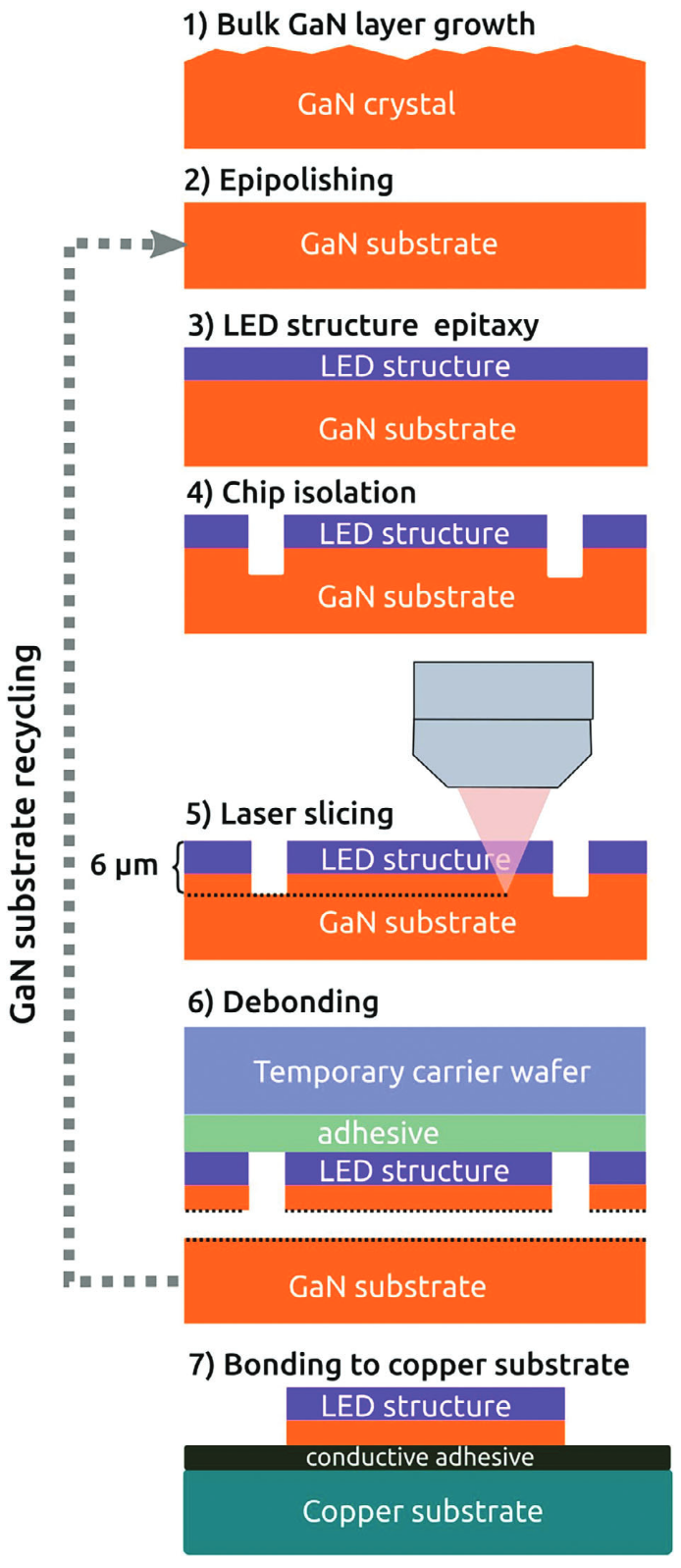
LLO processes a millimeter-scale spot per pulse and can release a six-inch GaN wafer in minutes. It is noncontact and avoids wet-chemical contamination. The trade-offs are thermal damage, a preference for transparent growth substrates, and the capital and maintenance cost of excimer equipment.
It is nevertheless a mature enabling process for GaN LEDs, Micro-LEDs, and flexible RF devices. Hybrid approaches with carbon nanotubes and other absorbing interlayers can improve thermal localization.
Mesoporous-layer-assisted exfoliation
Mesoporous-layer-assisted exfoliation inserts a porous Si, porous GaN, or similar intermediate layer whose high surface area and controlled corrosion weaken the interface.
- Form pores with electrochemical or chemical etching, typically 2–50 nm in diameter and 30–70% porosity.
- Grow the single-crystal functional layer above the porous region.
- Dissolve or weaken the porous layer with KOH, HF, or another selective chemistry.
- Transfer the film by rolling, vacuum pickup, or van der Waals adhesion.
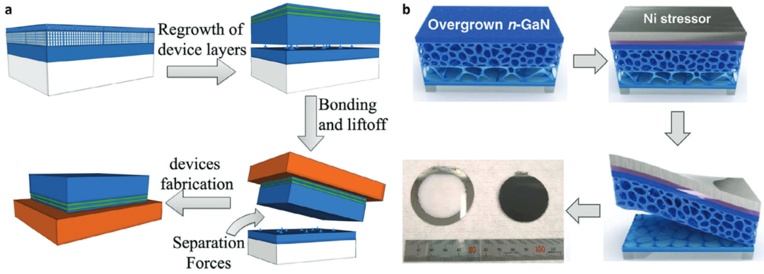
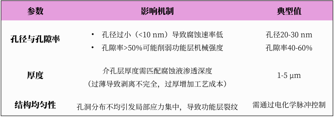
The porous structure concentrates stress, provides rapid etchant paths, and mechanically cushions shear during release. Porous silicon can etch near 500 nm/min, reducing release time from hours to minutes. Because no laser or high-temperature release step is required, the method is compatible with heat-sensitive organics and perovskites and with opaque carriers. The main challenges are the complexity of porous-layer preparation and defects inherited by the overgrown film.
Two-dimensional-material-assisted exfoliation
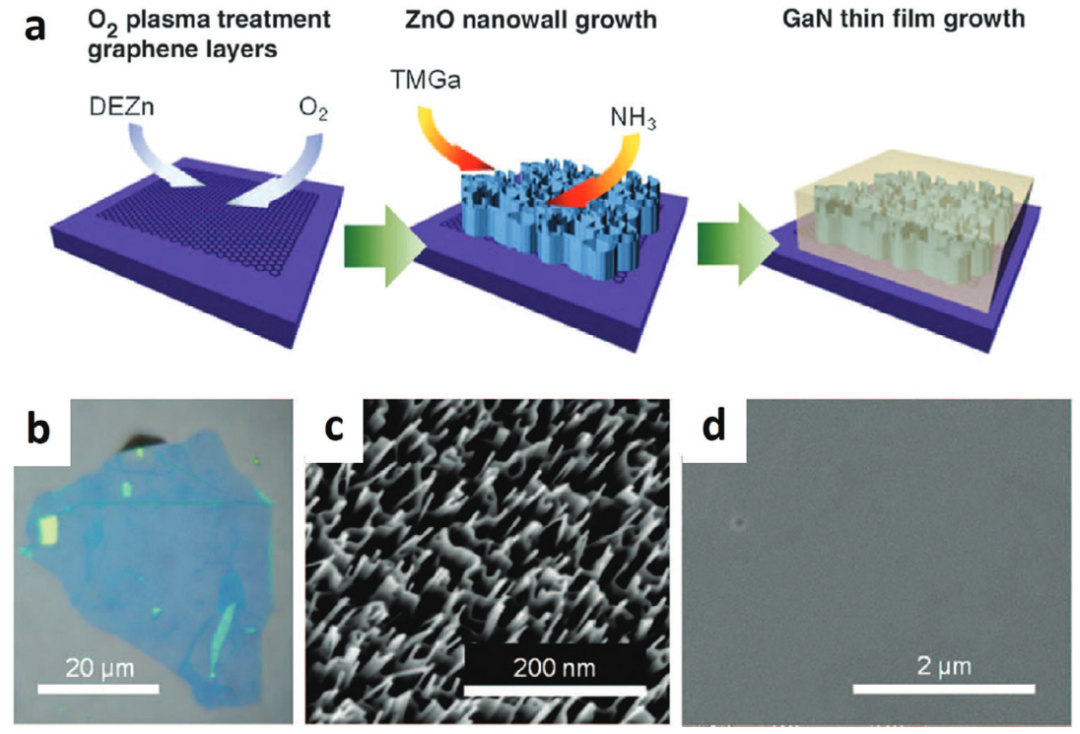
Graphene, hexagonal boron nitride, and transition-metal dichalcogenides provide atomically smooth, weakly bonded interfaces. A functional film can be grown over them and then released mechanically, chemically, or with a thermal-release tape before transfer with PDMS, PVA, or direct van der Waals bonding.
- Graphene: conductive and ultrathin, suitable when a transparent electrode or conducting interface is useful.
- h-BN: electrically insulating and thermally stable above 1000 °C.
- MoS₂: a semiconductor with a monolayer-scale band gap near 1.8 eV, usable as either a functional or release layer.
The main advantage is broad heterogeneous-integration freedom because strong lattice matching is no longer required. Material cost, defect control, and wafer-scale growth remain industrial barriers.
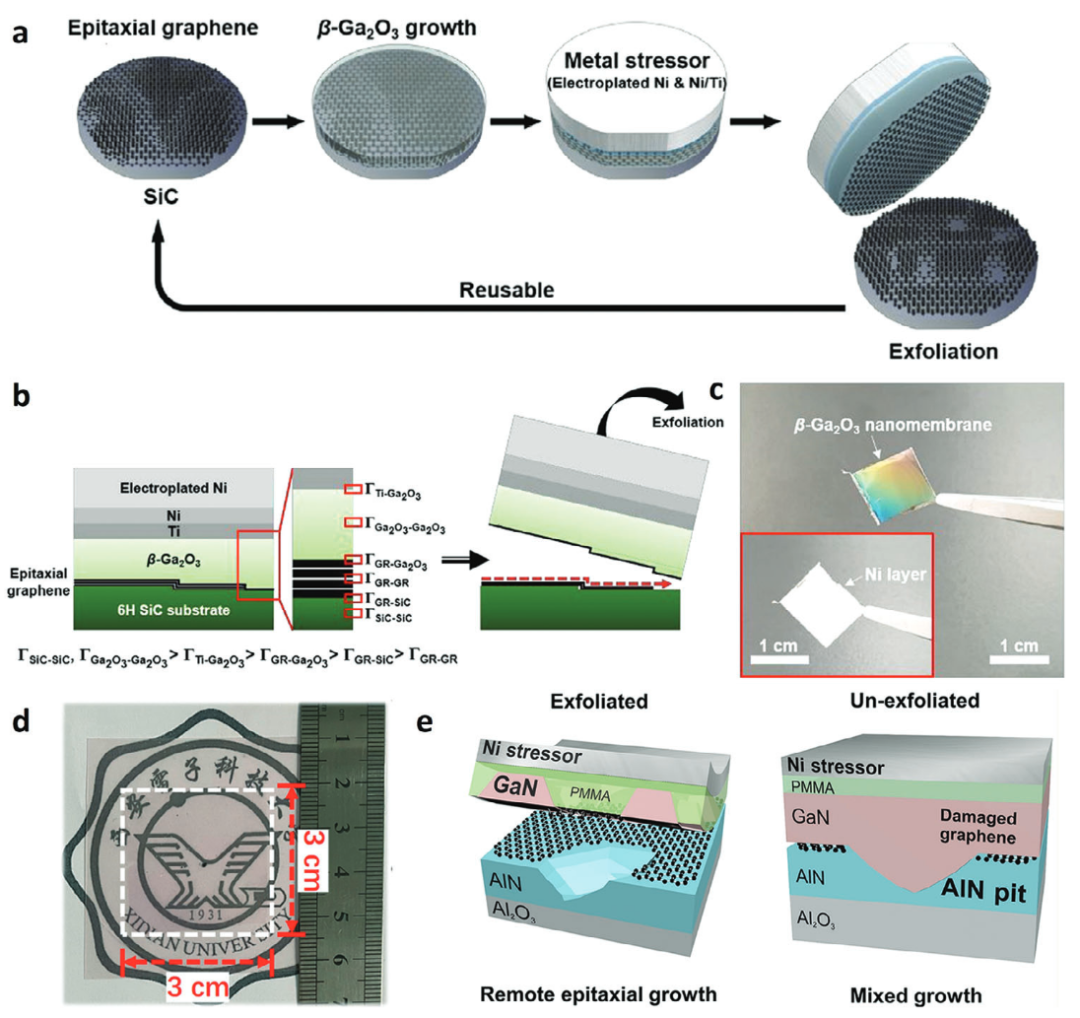
Applications in optoelectronics and power electronics
LEDs
InGaN LED layers can be transferred from their growth wafer to silicon, plastic, and other platforms while retaining emission and enabling flexible or deformable arrays.
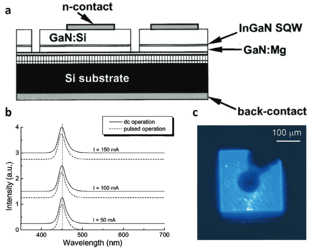
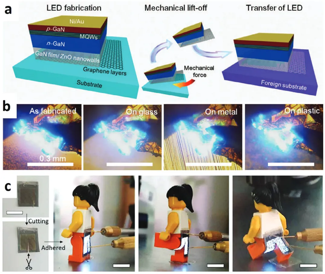
Photodetectors
Released Ga₂O₃ and related wide-band-gap membranes support vertical, flexible, and self-powered ultraviolet photodetectors.
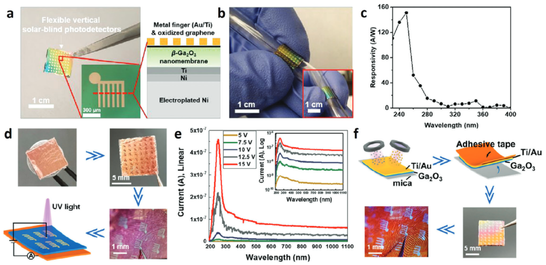
MESFETs and HEMTs
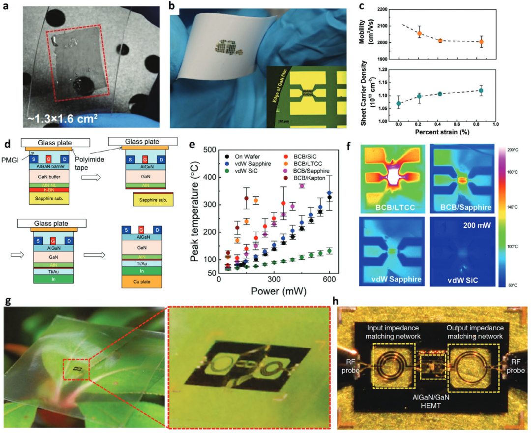
Transferred high-electron-mobility devices combine high-quality epitaxy with flexible RF circuits and improved thermal management on a selected target substrate.
Reference
- Hongliang Chang et al., “Semiconductor Membrane Exfoliation: Technology and Application”, Advanced Electronic Materials, 11.1 (2025), 2300832. DOI: 10.1002/aelm.202300832.
The original Chinese edition was published by “Laser Insights” in Chongqing on March 7, 2025. View the original post. This page preserves the technical content, parameters, figures, conclusions, and reference in a web-native structure.