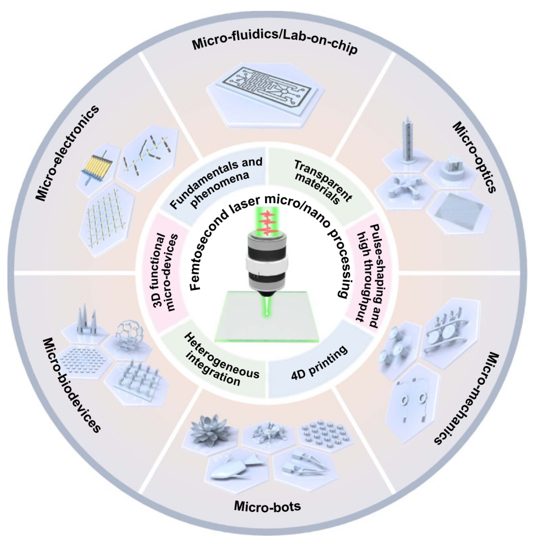
Femtosecond laser micro- and nanofabrication links ultrafast energy deposition to transparent-material modification, three-dimensional polymerization, pulse shaping, parallel processing, and functional device integration. This article follows that path from physical mechanisms to applications.
Ultrafast interaction Transparent materials Two-photon polymerization 3D / 4D microfabrication
Application background
A femtosecond laser produces pulses with durations on the order of femtoseconds, where \(1\ \mathrm{fs}=10^{-15}\ \mathrm{s}\). Its combination of extremely short duration and very high peak power creates four core capabilities:
Interaction ends before picosecond-scale thermal relaxation, minimizing the heat-affected zone.
Even transparent materials absorb through multiphoton and tunneling ionization.
A focus can be positioned inside transparent matter to create buried 3D structures.
The process can create LIPSS, nanogratings, color centers, and nanocrystals.
In “cold” processing, the pulse ends before electron–phonon coupling and other thermal-relaxation processes spread energy. Material can therefore be modified or removed with little melting, recast, or cracking. Nonlinear absorption also removes the normal wavelength-selectivity constraint, allowing metals, semiconductors, dielectrics, polymers, and biological tissues to be processed with one broadly adaptable platform.
Representative applications include:
- Microelectronics and photonics: waveguides, photonic crystals, microresonators, integrated optical circuits, and sensors.
- Micro- and nanoelectromechanical systems: microsensors, actuators, and micromotors.
- Biomedicine: microfluidic chips, drug-delivery systems, tissue-engineering scaffolds, biosensors, and microneedle arrays.
- Functional materials and surfaces: superhydrophobic or superhydrophilic surfaces, antireflection textures, and catalytic structures.
- Data storage: five-dimensional optical storage.
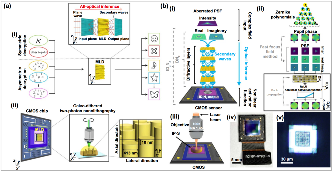
- AI photonics: optical neural networks and photonic computing units.
Femtosecond laser–matter interaction
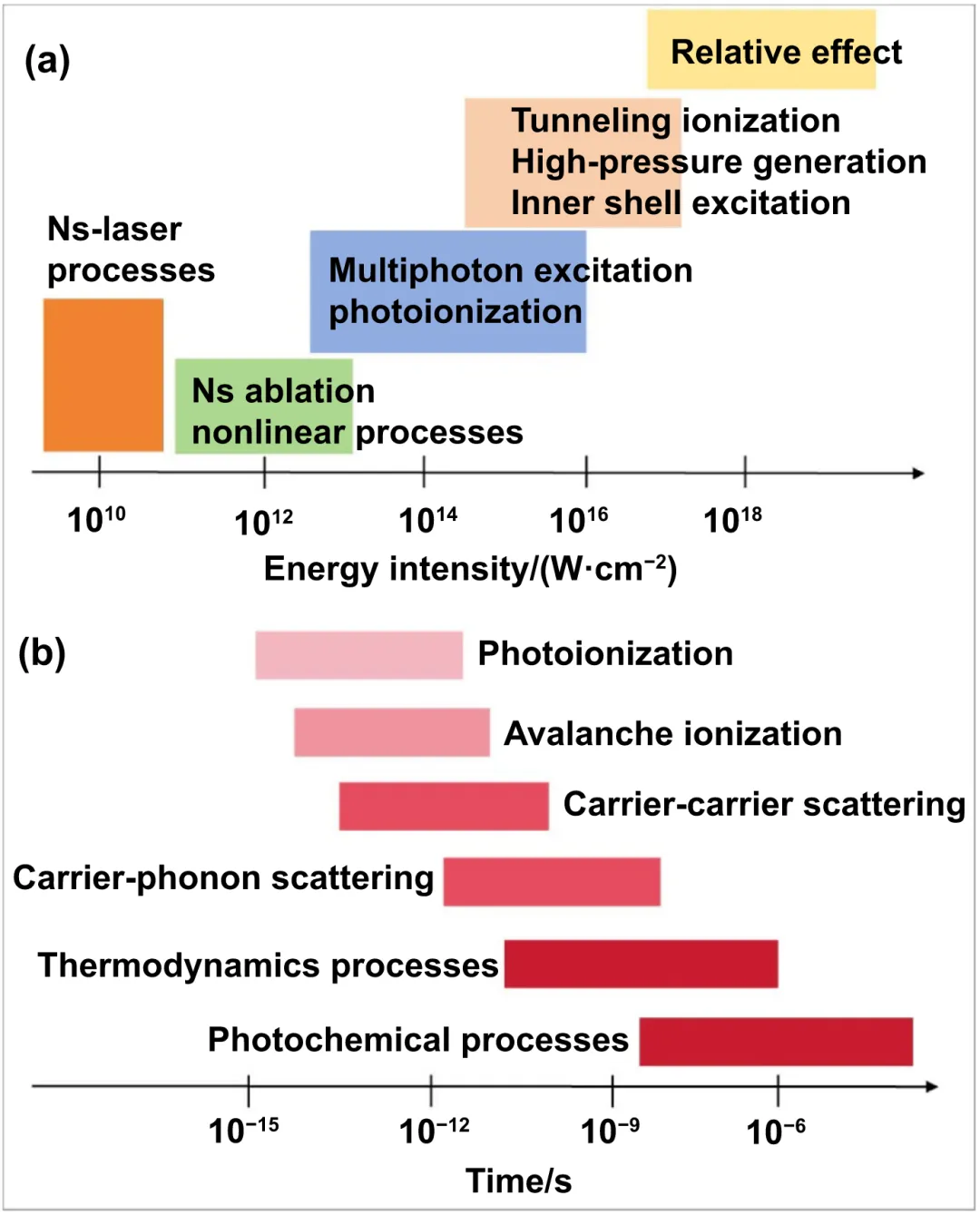
- Femtosecond scale: the field excites optically active electronic states, causing electron heating, electronic nonequilibrium, nonthermal phase transitions, and Coulomb explosion.
- Picosecond scale: excited electrons transfer energy to atomic motion, and nonequilibrium transformations such as homogeneous melting develop.
- Nanosecond scale: the irradiated zone cools and solidifies; heterogeneous melting, melt flow, resolidification, and microstructural modification dominate.
Ionization mechanisms
The central feature of femtosecond interaction is its nonlinearity: photons are concentrated into a very short time and a small focal volume.
- Multiphoton ionization: an electron absorbs several photons nearly simultaneously and reaches the conduction band. This is especially important in transparent materials.
- Tunneling ionization: a strong electric field bends and narrows the Coulomb barrier, allowing a bound electron to tunnel into a free state.
- Avalanche ionization: existing free electrons gain energy from the field and collisionally ionize additional bound electrons, creating a multiplying cascade.
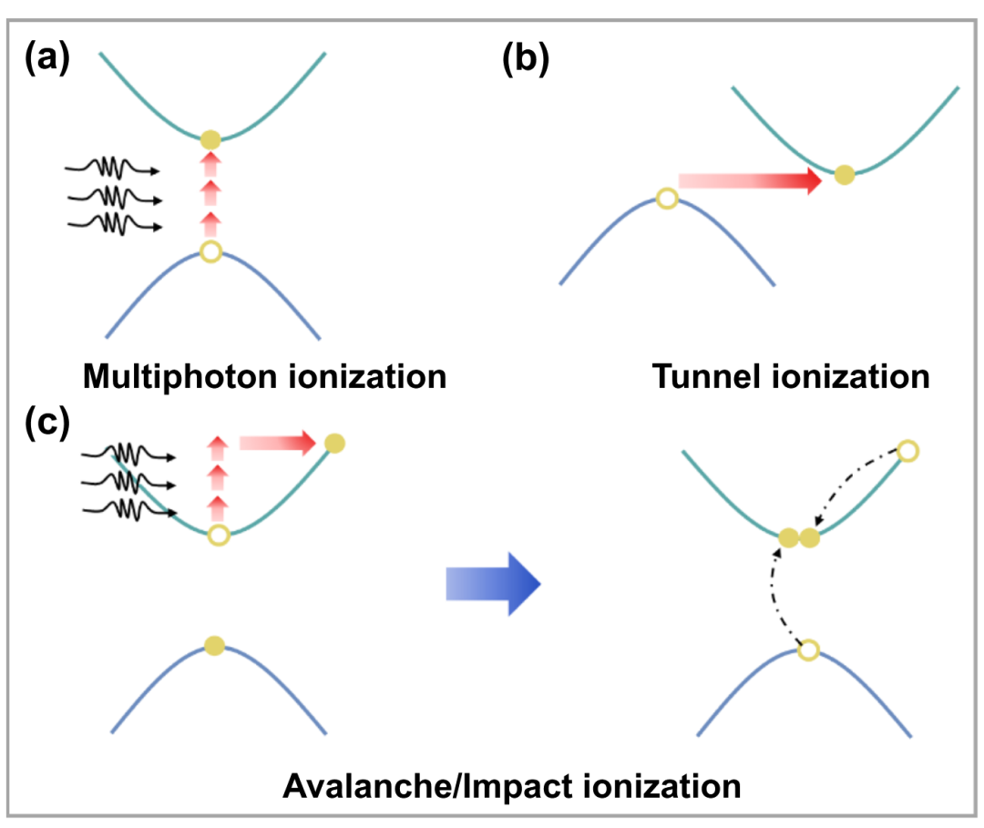
Energy transfer and phase transformation
- Metals: free electrons absorb photons and heat rapidly, then transfer energy through electron–electron collisions and electron–phonon coupling, raising lattice temperature and causing melting or vaporization.
- Nonmetals: dielectrics and semiconductors first generate free carriers through ionization. The carrier plasma absorbs additional energy and later transfers it to the lattice.
- Nonthermal melting and ablation: strong electronic excitation destabilizes the lattice before conventional thermal equilibrium is reached. This is one physical basis of cold processing.
- Thermal melting and ablation: energy reaches the lattice through electron–phonon coupling and drives familiar melting, vaporization, and removal.
- Coulomb explosion: rapid electron removal leaves a positively charged surface whose ion–ion repulsion ejects material explosively.
- Photomechanical spallation and phase explosion: confined pressure creates voids and layer separation, or superheated matter decomposes explosively near a critical state.
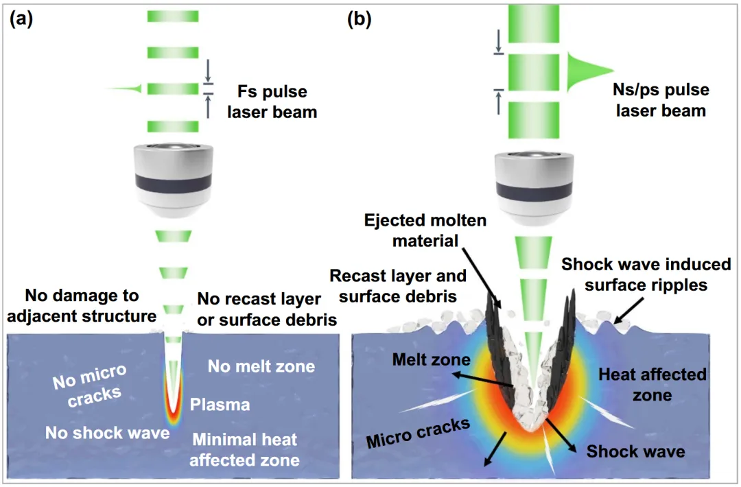
Physical modification by femtosecond pulses
Surface modification
- Laser-induced periodic surface structures (LIPSS): periodicity is usually near or below the wavelength. Interference between incident light and surface plasmon polaritons or scattered waves creates textures that tune reflection, structural color, wetting, and friction.
- Light-trapping structures: micro- and nanotextures on silicon and other absorbers can increase optical path length and improve solar-cell absorption.
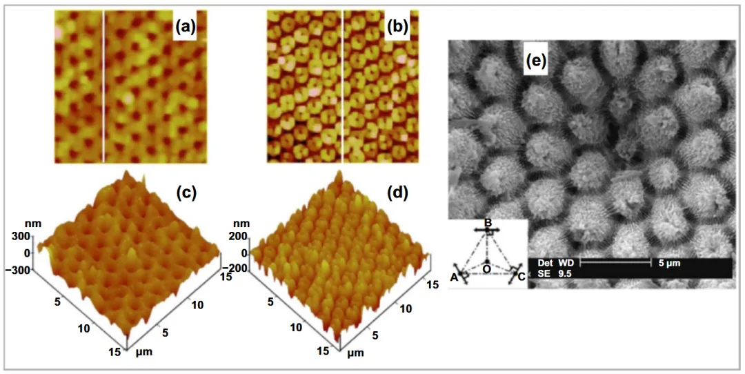
Bulk modification
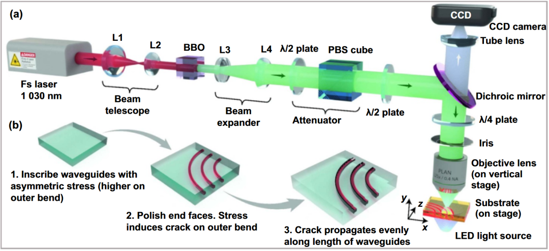
- Refractive-index change: supports waveguides and gratings in transparent media and may appear as smooth index increase, birefringent nanogratings, or microvoids.
- Crystallization: localized heating and rapid cooling alter the crystalline state.
- Microvoids and microchannels: high-energy focusing produces a confined microexplosion inside transparent matter, enabling buried fluidic channels and cavities.
Microscale removal and deposition
Nanosecond drilling is often limited by poor edge quality, stress cracking, recast layers, and fragmentation. Femtosecond pulses strongly limit heat diffusion and control deposition more precisely, producing high-resolution features with fewer defects. Cutting and scribing are particularly valuable for hard brittle materials such as semiconductors, glass, and sapphire.
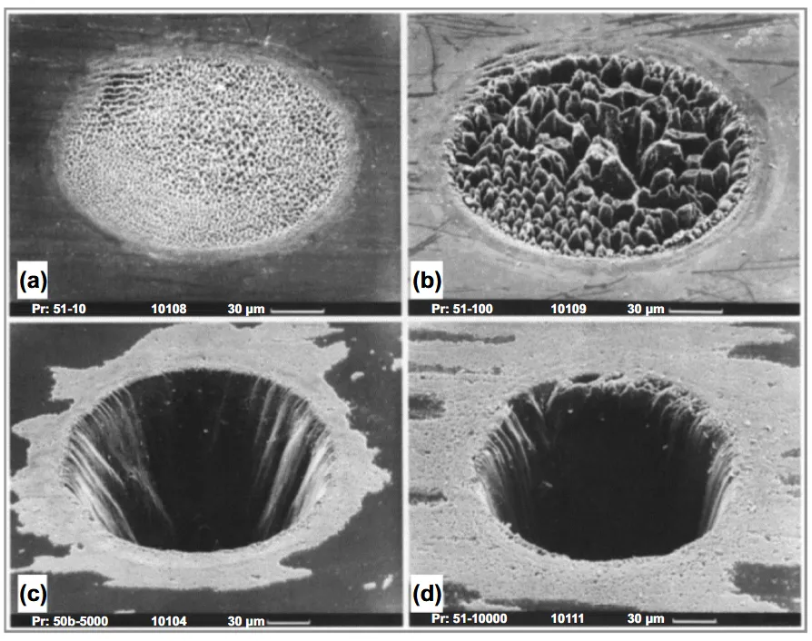
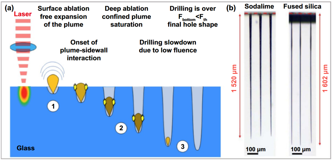
In deposition, a femtosecond pulse ablates a target and the ejected species condense on another substrate as a thin film or nanoparticle layer.
Two-photon polymerization and photochemistry
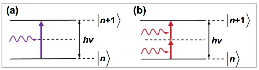
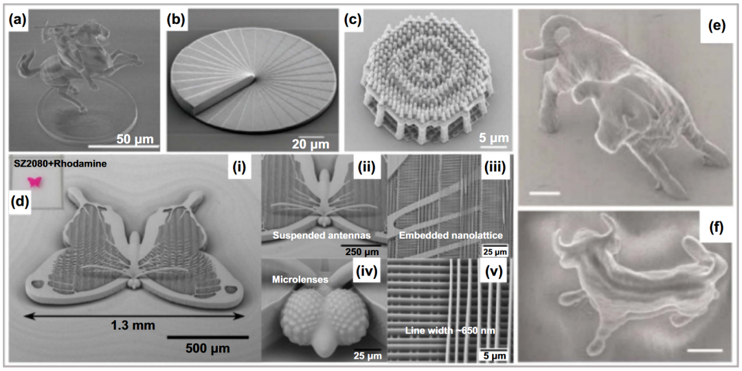
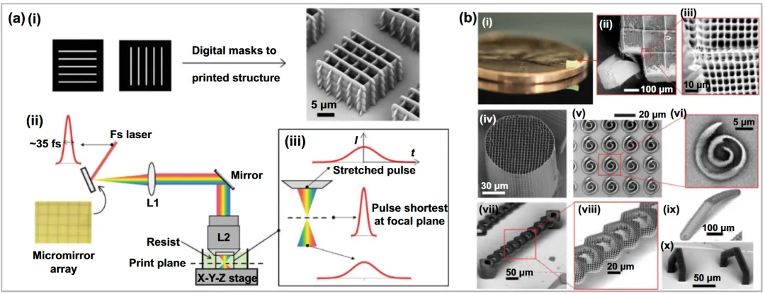
Two-photon polymerization (TPP), also called two-photon lithography, is a major additive-manufacturing use of femtosecond lasers. A photoinitiator absorbs two or more photons and triggers polymerization, so liquid resin solidifies only within the focal voxel. Because two-photon probability scales approximately with the square of intensity, curing is tightly localized and true three-dimensional features below the diffraction-limited focal size can be produced.
The main advantages are free-form 3D fabrication and high resolution, with feature sizes reaching hundreds or tens of nanometers under optimized conditions.
Other induced phenomena
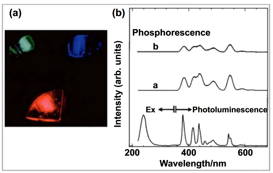
Photoluminescence: ultrafast writing can generate upconversion fluorescence and persistent afterglow in rare-earth-doped glass and crystals.
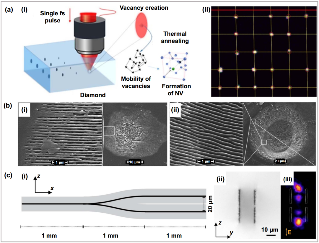
Color centers: femtosecond modification can create nitrogen-vacancy centers in diamond, which are important building blocks for quantum sensing and quantum information.
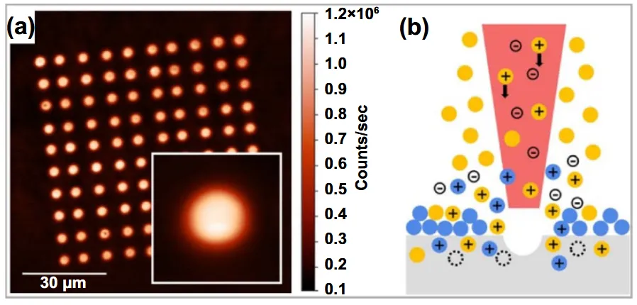
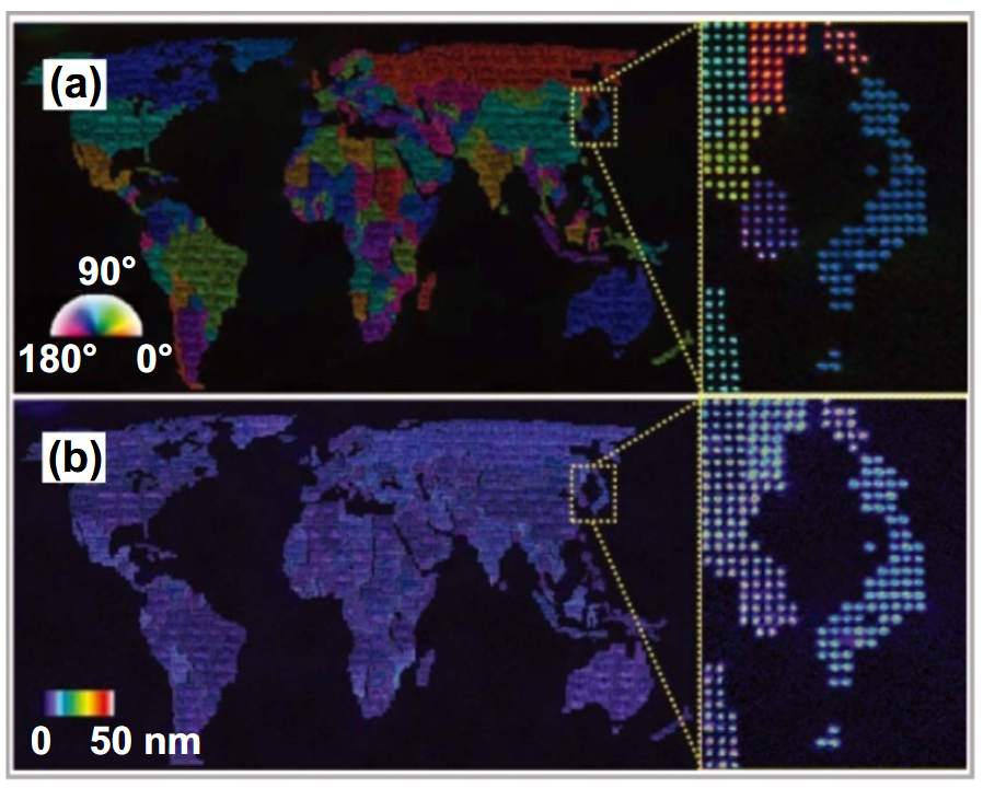
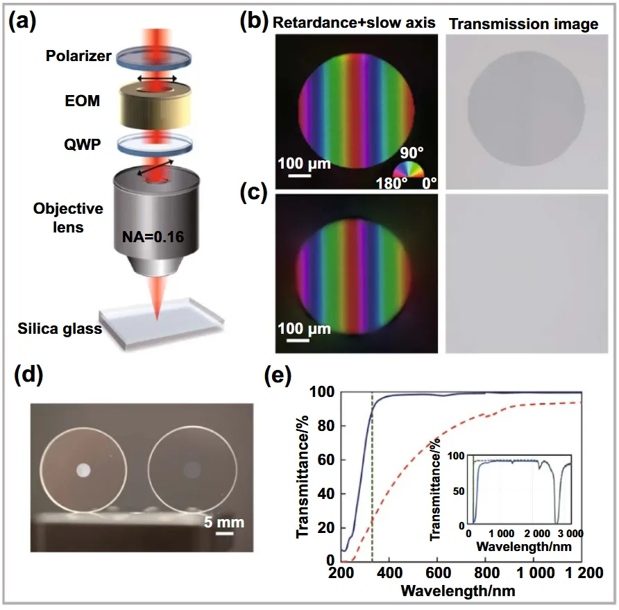
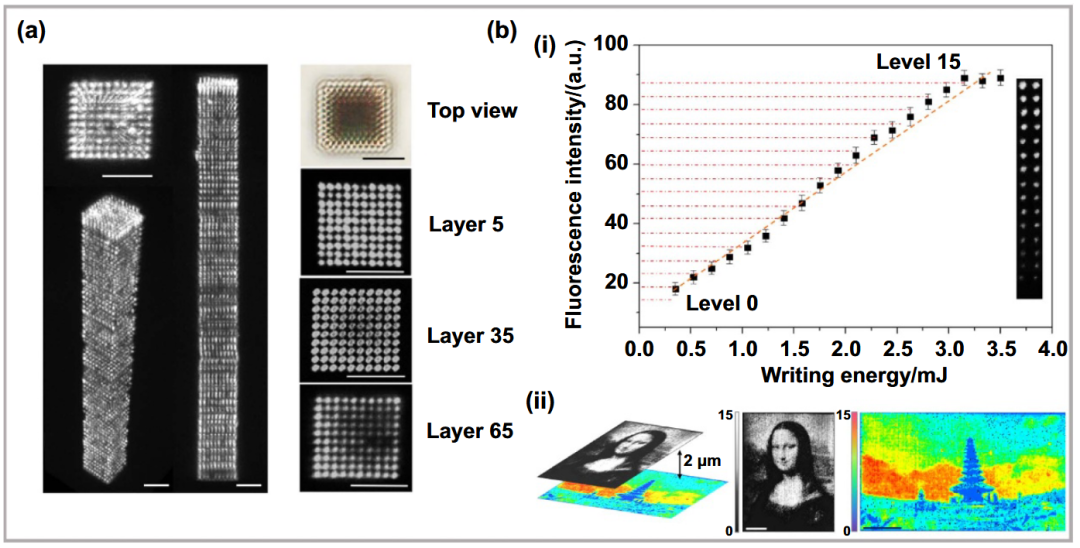
Nanogratings: periodic nanoscale structures written inside transparent materials are birefringent and can serve polarization optics, data storage, and sensors.
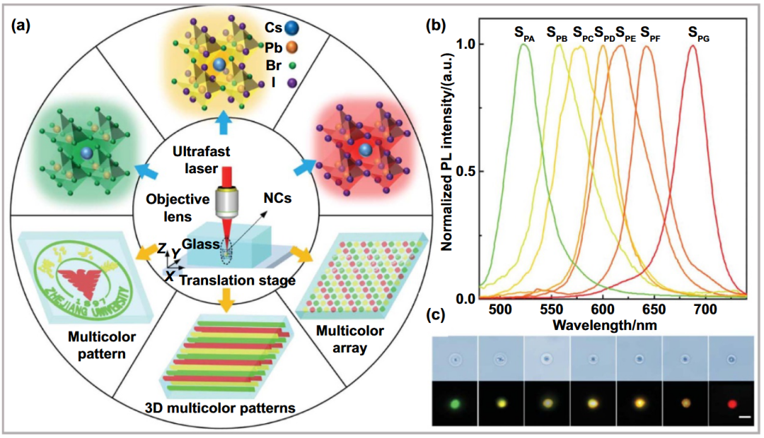
Nanocrystals: localized high temperature and pressure can nucleate perovskite and other nanocrystals in glass for emitters, solar cells, and optical data storage.
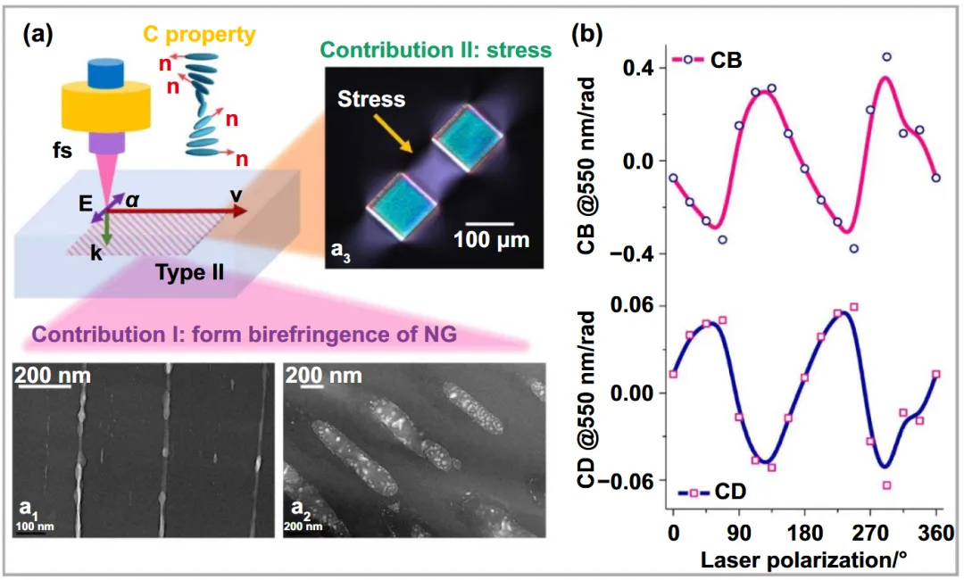
Tailored optical properties: processing parameters can induce controllable optical chirality even in initially achiral materials such as silica.
Micro- and nanofabrication of transparent materials
Glass and fused silica
Glass is among the most widely processed materials because of its optical transparency and chemical stability. Different modification regimes can form buried channels, volume gratings, and waveguides. Fused silica, with its high damage threshold and excellent ultraviolet transmission, is a benchmark material for femtosecond research and applications.
Polymers
Polymers require relatively little processing energy, are inexpensive and formable, and can be chemically doped. They support optical storage, microchannels, gratings, and waveguides. TPP in polymers is highly mature, although thermal stability and mechanical strength can be lower than in glass or crystals.
Diamond, sapphire, and functional crystals
Diamond: femtosecond lasers can create NV centers, waveguides, microfluidic structures, and quantum sensors. Processing is difficult, but diamond’s hardness, thermal conductivity, wide band gap, and biocompatibility make it valuable in extreme environments and quantum technology.
Sapphire: high hardness, thermal stability, and transparency make it an important optical and substrate material, but uncontrolled processing can readily generate cracks.
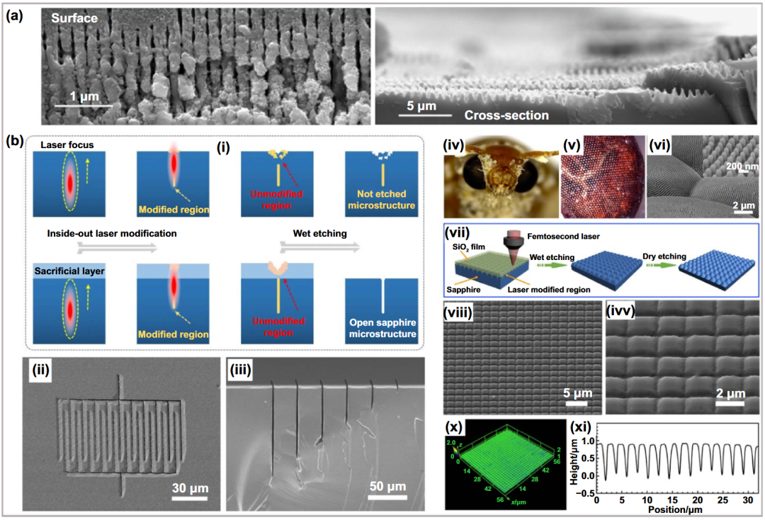
Functional crystals: YAG, Nd:YAG, LiNbO₃, quartz, and TeO₂ can host nanostructures, waveguides, index-modified zones, birefringent regions, and microholes. LiNbO₃ is especially important for electro-optic, acousto-optic, and nonlinear-optical devices; direct-written waveguides and periodic structures add new functionality without conventional wafer processing.
Gels, liquids, and photoresists
TPP commonly uses liquid or gel photoresists:
- Negative resists: irradiated regions cross-link and remain after unexposed material is washed away. Examples include acrylates, SU-8 epoxy, Ormocer® hybrid sol–gels, and SZ2080.
- Positive resists: irradiation makes exposed material soluble so it is removed during development.
- Critical properties: transparency, two-photon absorption cross-section, polymerization shrinkage, mechanical strength, and biocompatibility.
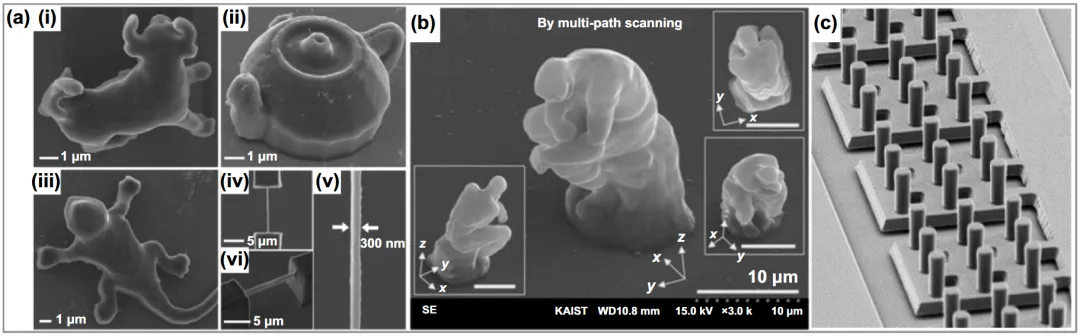
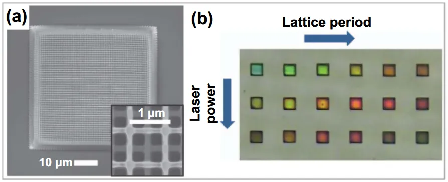
Pulse shaping and high-throughput processing
Femtosecond pulse shaping
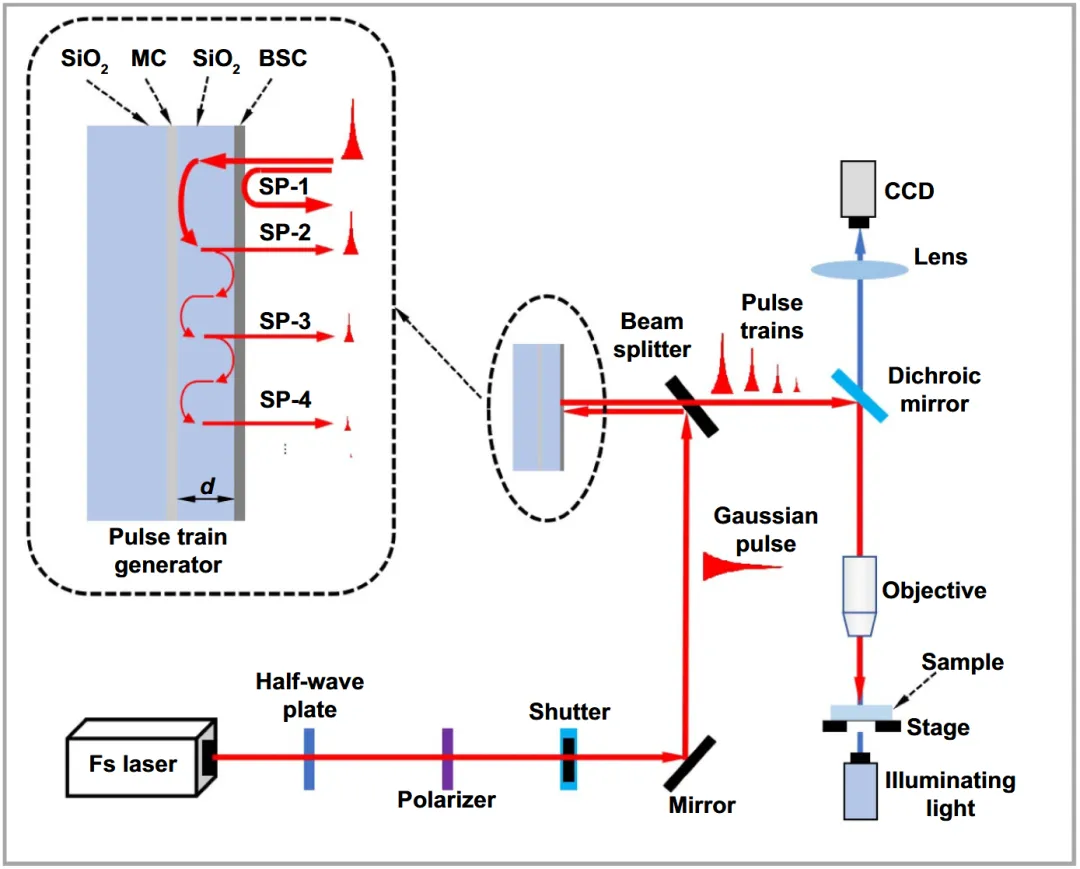
Temporal shaping controls how energy is distributed in time. Pulse trains can improve removal efficiency, reduce heat accumulation, and tune quality. Implementations include beam splitters, acousto-optic modulators, Fourier-domain pulse shapers, and thin-film resonators.
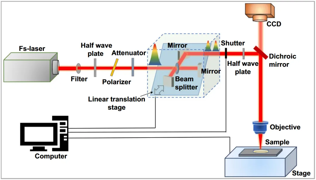
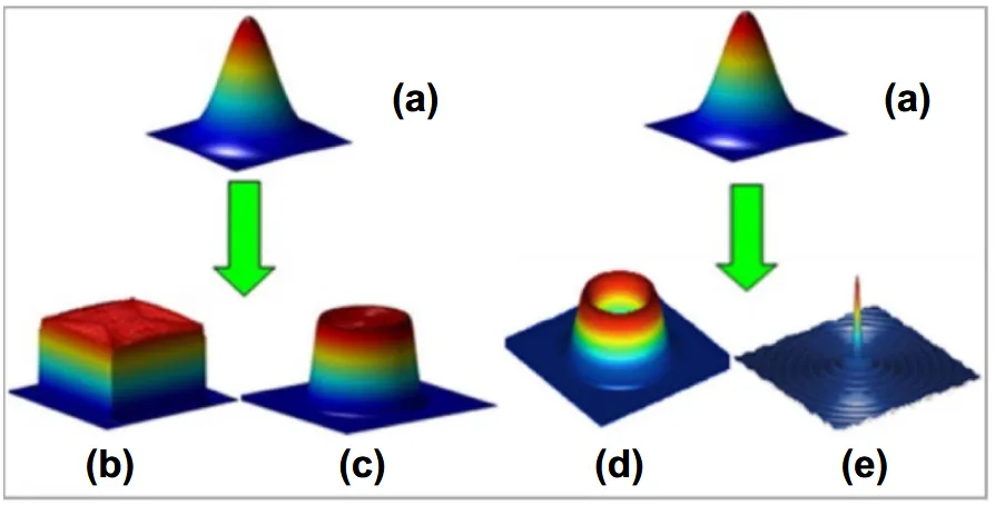
Spatial shaping changes the transverse energy distribution to form flat-top, Bessel, or vortex beams. Diffractive optical elements, birefringent lens groups, and spatial light modulators are common tools.
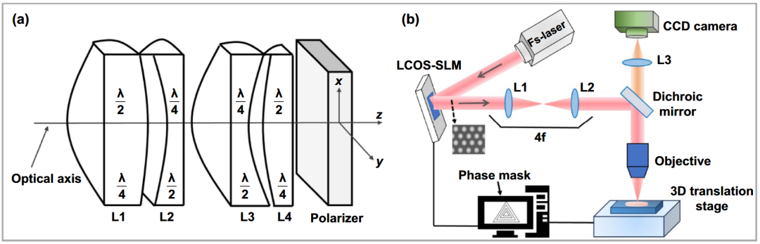
Frequency shaping changes wavelength through nonlinear processes such as second-harmonic generation and optical parametric amplification.
Pulse shaping expands the process window. Temporally shaped bursts can improve glass cutting and drilling; spatial shaping, especially Bessel beams and programmable SLMs, increases depth tolerance, parallelism, and three-dimensional flexibility.
High-throughput femtosecond processing
Point-by-point scanning is inherently slow. Three strategy families increase throughput:
- Source and motion improvements: higher average power, higher repetition rate, faster galvanometers, and more accurate stages.
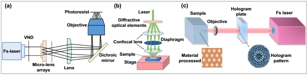
- Multifocus and multi-beam interference: microlens arrays or diffractive optics generate many foci, while interference creates periodic patterns over a large area.
- Holographic pattern processing: an SLM or DMD displays a computed hologram and projects a target pattern for area-wise exposure.
4D printing and nanoscale resolution
Micro- and nanoscale 4D printing
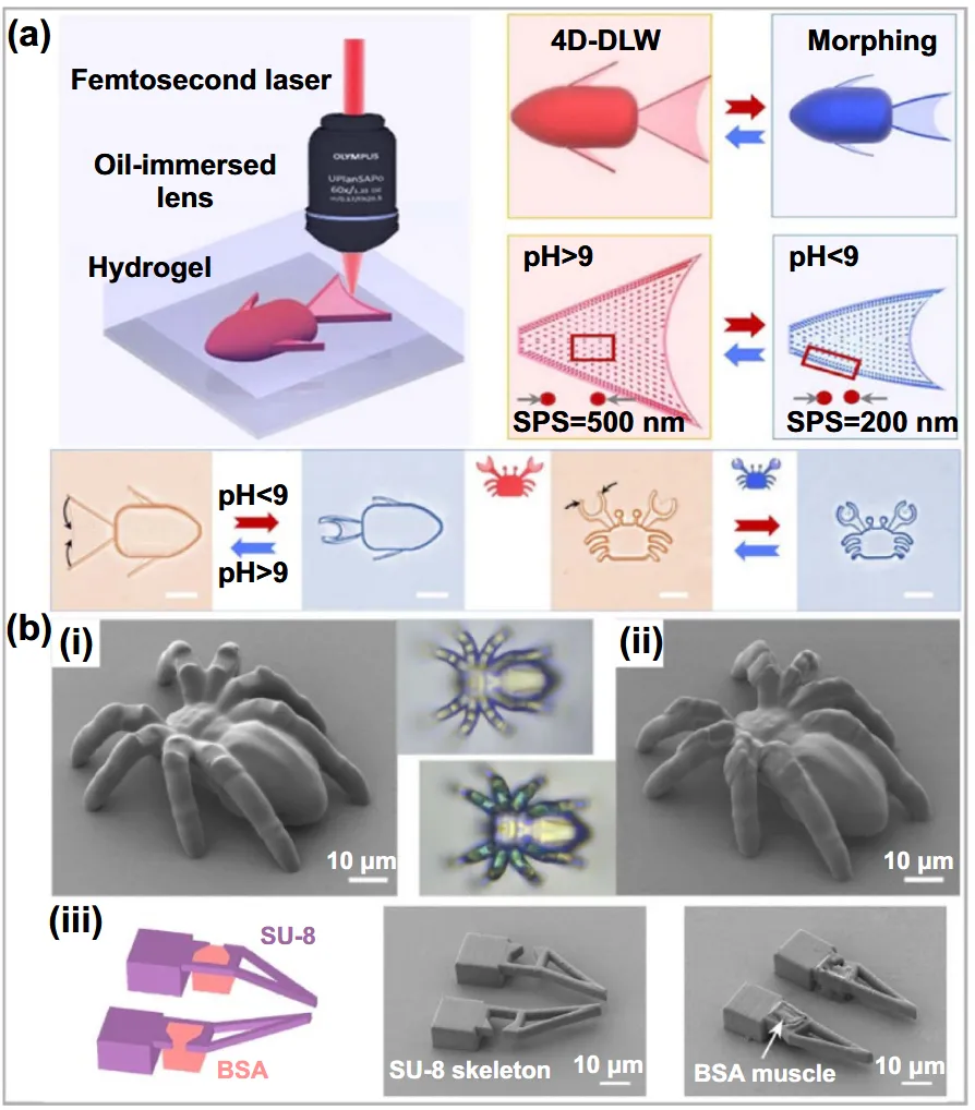
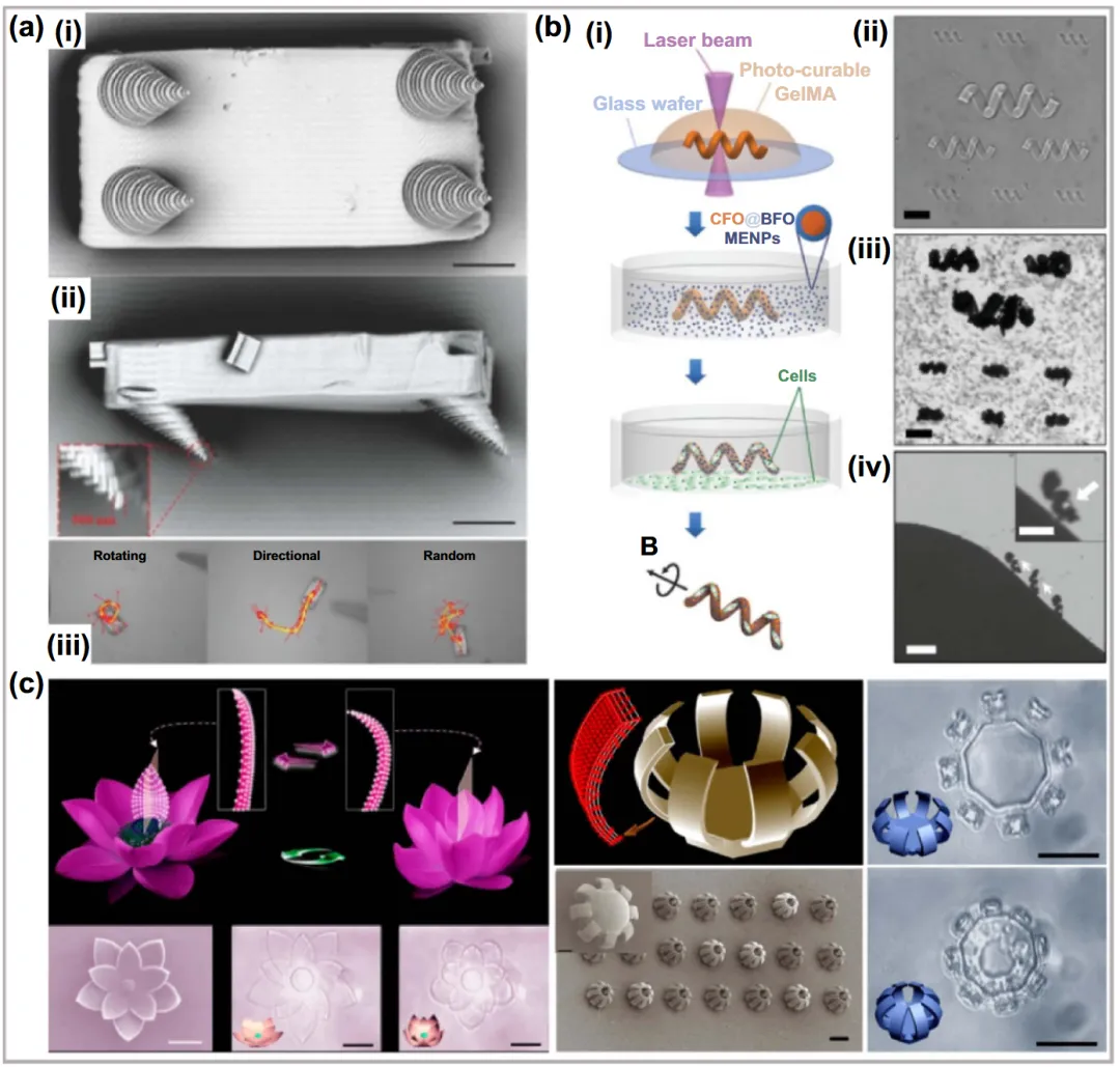
4D printing combines a printed 3D structure with time-dependent response. The structure changes shape, properties, or function under temperature, pH, light, magnetic field, solvent, or another stimulus.
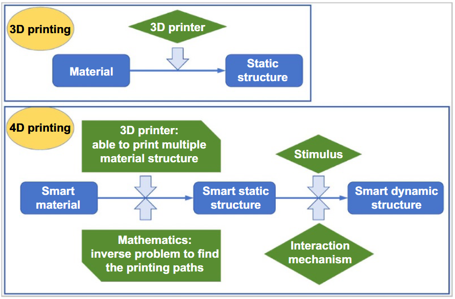
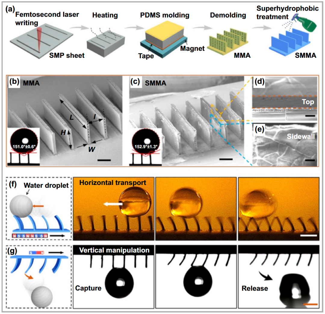
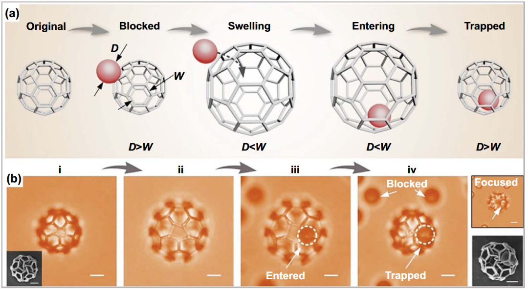
These systems point toward reconfigurable microdevices for soft robotics, biomedical tools, and adaptive sensors.
Super-resolution nanofabrication
The goal is to move beyond the conventional diffraction limit toward features of tens of nanometers or, in specialized demonstrations, only a few nanometers. Two different metrics matter: linewidth, the smallest feature that can be produced, and writing resolution, the smallest spacing at which two adjacent features remain distinct.
- Near-field methods: adaptive scanning probes, near-field optical microscopy, and microsphere-assisted processing provide very high resolution but operate close to a surface.
- Far-field threshold control: TPP can confine polymerization by tuning power, exposure, scan speed, initiator sensitivity, and diffusion so only the highest-intensity core crosses threshold.
- STED-inspired lithography: a Gaussian excitation beam initiates polymerization while a doughnut-shaped depletion beam suppresses the excited state around it, shrinking the effective voxel.
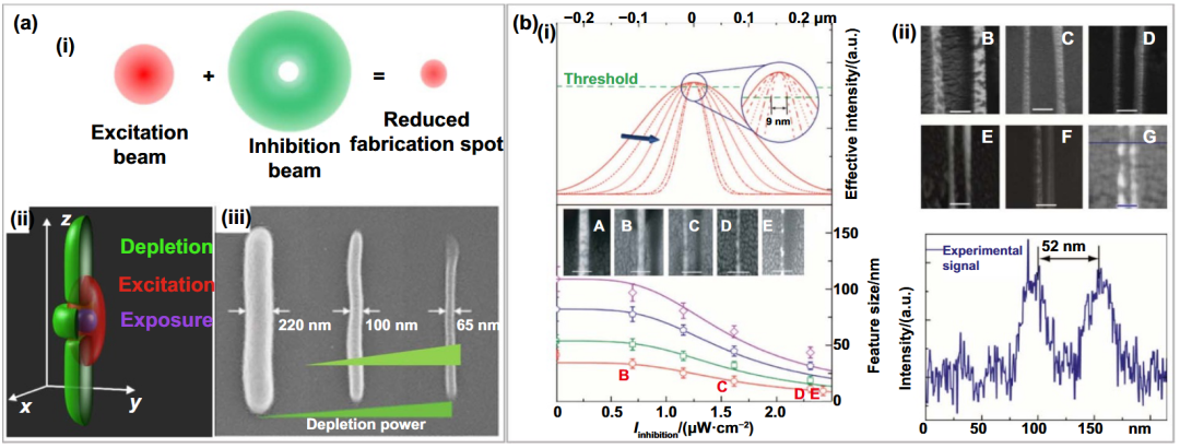
Heterogeneous integration of functional materials
Heterogeneous integration combines materials and components with different functions in one device, creating capabilities that no single material can provide. It is especially important in photonic integrated circuits.
- Monolithic integration: for example, epitaxial growth of compound semiconductors on silicon.
- Hybrid integration: bonding and assembling separately optimized components.
- Pulsed laser deposition: ablating a source target and depositing the vapor on a receiving substrate.
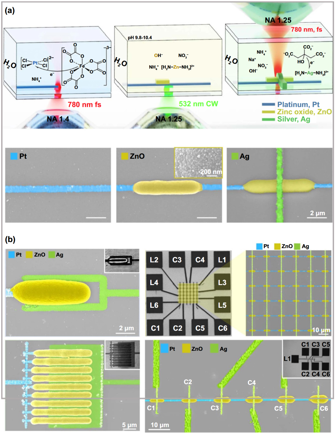
- Femtosecond direct writing: writing waveguides and interconnects inside bulk material to connect existing structures.
- Van der Waals integration: stacking two-dimensional materials or nanomembranes with weak interfacial bonding and relaxed lattice-matching requirements.
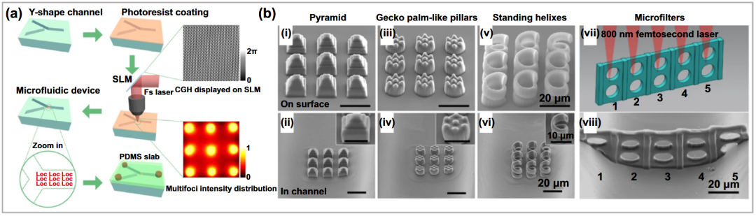
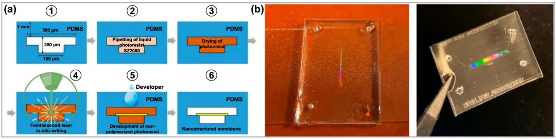
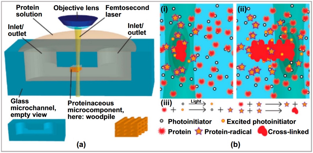
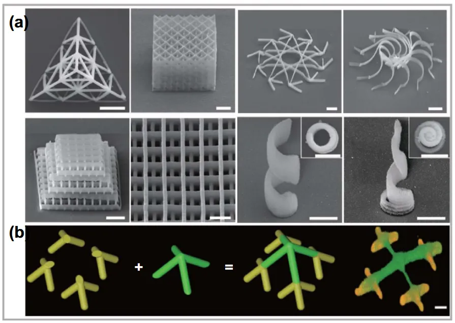
Applications in three-dimensional functional microdevices
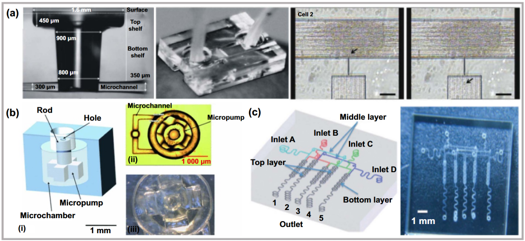
Microfluidic chips
Femtosecond-assisted etching and water-assisted drilling can create complex three-dimensional lab-on-chip structures.
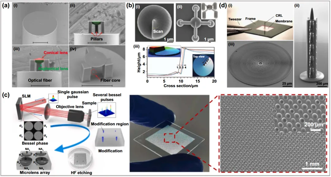
Micro-optics
The process can form microlenses, micro-waveplates, and three-dimensional photonic crystals.
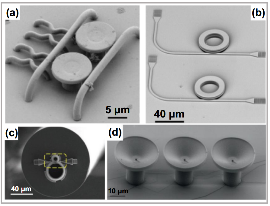
Micromechanics
Direct writing supports microresonators, compliant structures, and actuators.
Microrobots
Many microrobots are 4D-printed structures whose geometry and material response convert external fields into motion.
Microelectronics
Femtosecond lasers can print flexible electronic devices, sensors, electrodes, and heterogeneous circuit elements.
Biomedical microdevices
- Microneedle arrays: support minimally invasive drug delivery, vaccination, and biofluid sampling.
- Biological scaffolds: provide three-dimensional environments for tissue engineering and cell studies.
The source caption describes “various TPP-fabricated microneedle arrays and biomimetic cell scaffolds,” but the archived source contained an empty image container and no corresponding asset. The caption is retained without substituting an unrelated image.
Artificial-intelligence photonics
Photonic devices can perform AI operations with high bandwidth and potentially low energy consumption.
Ionization, plasma formation, and ultrafast energy transfer.
Ablation, direct writing, polymerization, shaping, and parallel exposure.
Optical, mechanical, electronic, biological, and intelligent integration.
Reference
- Gao, L., Zhang, Q., & Gu, M. “Femtosecond laser micro/nano processing: from fundamental to applications.” International Journal of Extreme Manufacturing, 7, 022010 (2025). DOI: 10.1088/2631-7990/ad943e.
The original Chinese edition was published by “Laser Insights” in Chongqing on May 23, 2025, at 07:26. View the original post