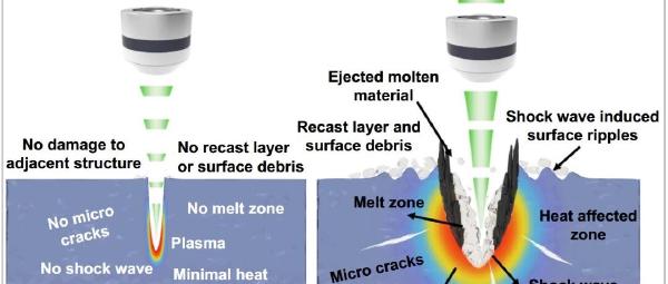
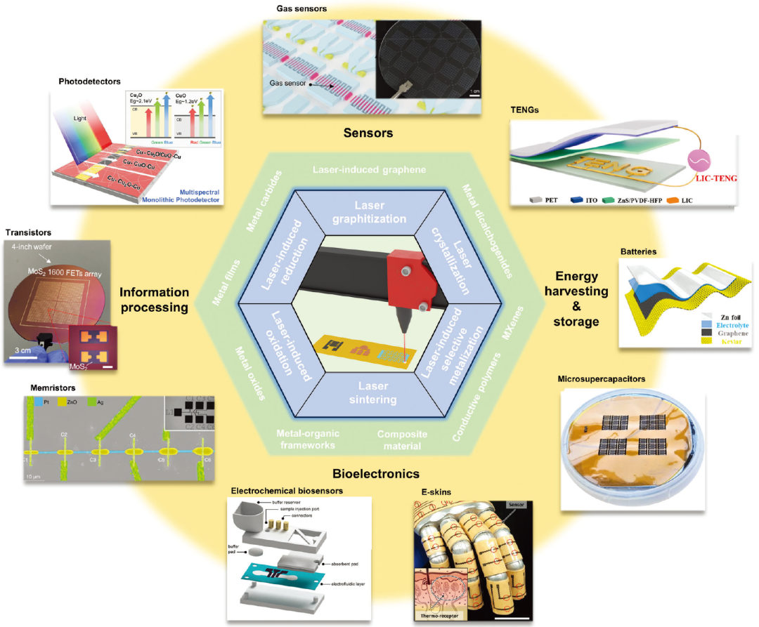
Direct laser writing now serves photodetectors, triboelectric generators, microsupercapacitors, transistors, memristors, flexible sensors, and bioelectronic devices. Its distinctive value is the ability to synthesize material, convert its phase or chemistry, and pattern a functional structure on one digitally controlled platform.
Direct laser writing Micro- and nanofabrication Material conversion Flexible electronics
Induced deposition, photopolymerization, and precursor conversion.
Reduction, oxidation, sintering, carbonization, and graphitization.
Selective ablation, lift-off, and microchannel machining.
Information, energy, sensing, and bioelectronics.
Application background
The Internet of Things, wearables, and flexible electronics require devices that bend, conform to complex surfaces, operate in harsh environments, and can be produced in many designs at modest volume. That creates three linked challenges: material compatibility, process adaptability, and manufacturing efficiency.
Photolithography and vapor deposition are mature but often require high temperature, vacuum, masks, and long multistep cycles. Organic semiconductors, polymer substrates, and nanocomposites may not tolerate those conditions, while small-batch IoT production cannot easily absorb high mask cost.
Alternative routes each solve part of the problem:
- solution processing supports low-temperature, large-area flexible substrates but struggles with high-resolution complex patterns;
- 3D printing reduces waste but depends on ink formulation and postprocessing;
- inkjet and other planar printing deposit multiple materials but are limited in resolution and structural freedom.
Direct laser writing (DLW) uses a focused beam and a digital toolpath to combine material synthesis, conversion, and patterning without a physical mask.
- Material compatibility: metals, polymers, organic semiconductors, and nanocomposites can be processed, and nanoparticles, dopants, or converted phases can be generated directly on the substrate.
- Process efficiency: a computer-defined path replaces a mask. Two-photon polymerization can make submicrometer 3D sensors, while ablation or sintering can create conductive traces rapidly.
The multi-material, high-resolution, and potentially low-energy character of DLW supports flexible electronics, quantum and photonic devices, biomimetic systems, and heterogeneous integration.
What is direct laser writing?
Definition
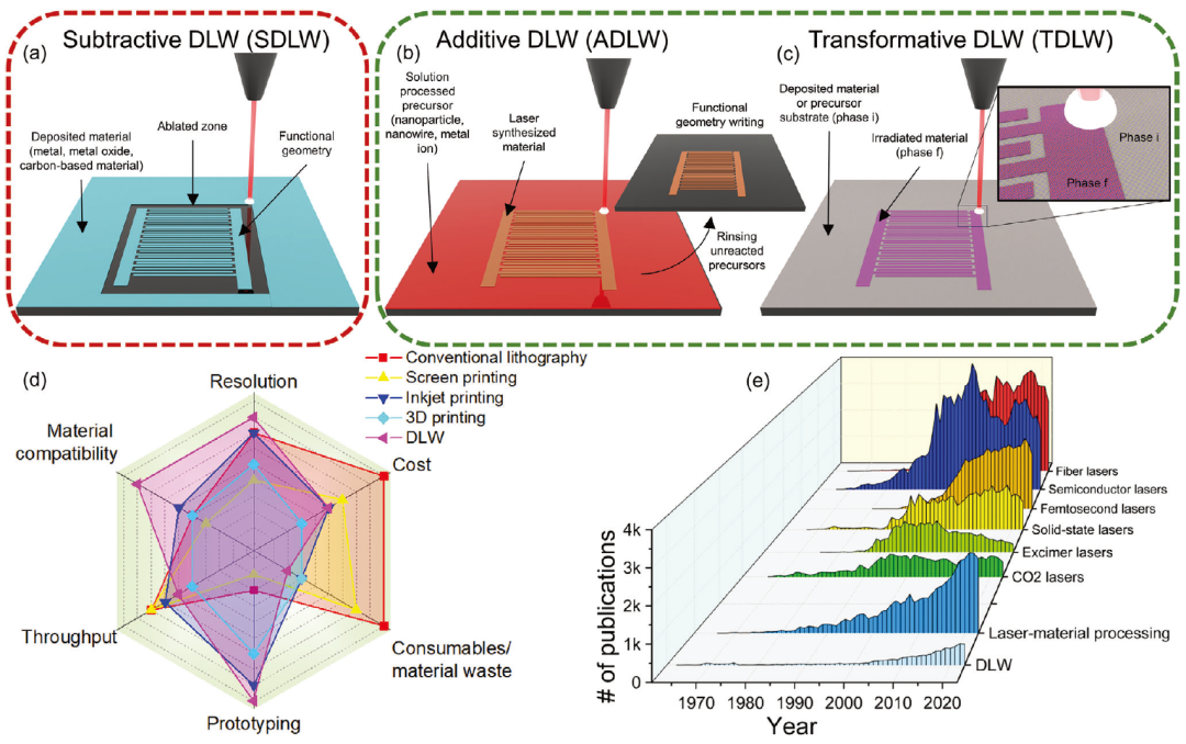
DLW is a maskless process in which a tightly focused beam interacts directly with a target to synthesize, convert, deposit, remove, or pattern material. Functional structures can be written at micrometer or nanometer scale without the mask alignment and repeated coating, exposure, and etching steps of conventional lithography.
Three process classes
Laser-induced deposition, photopolymerization, and solution-precursor conversion for conductors and 3D microstructures.
Reduction, sintering, graphitization, and phase conversion such as reduced graphene oxide, LIG, and oxide semiconductors.
Selective ablation and lift-off for circuit patterning and microfluidic channels.
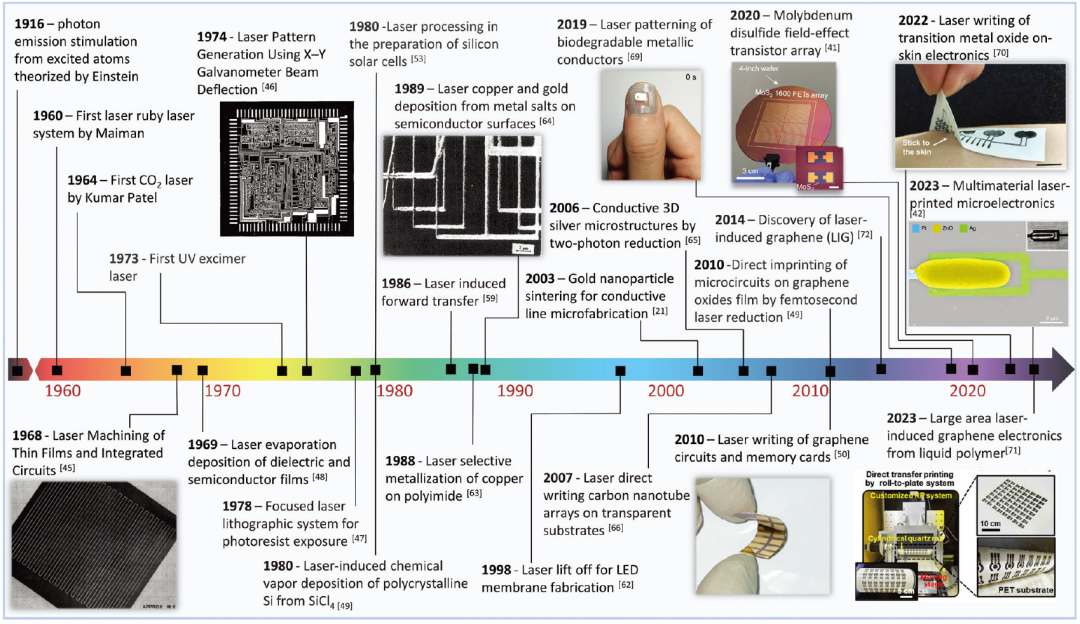
Laser processing in electronics has evolved from 1960s demonstrations, through IC trimming and mask patterning in the 1970s, laser lithography and annealing in the 1980s, pulsed-laser deposition in the 1990s and 2000s, laser-induced graphene and flexible electronics in the 2010s, and multi-material electronic printing in the 2020s.
Laser systems and key parameters
System architecture
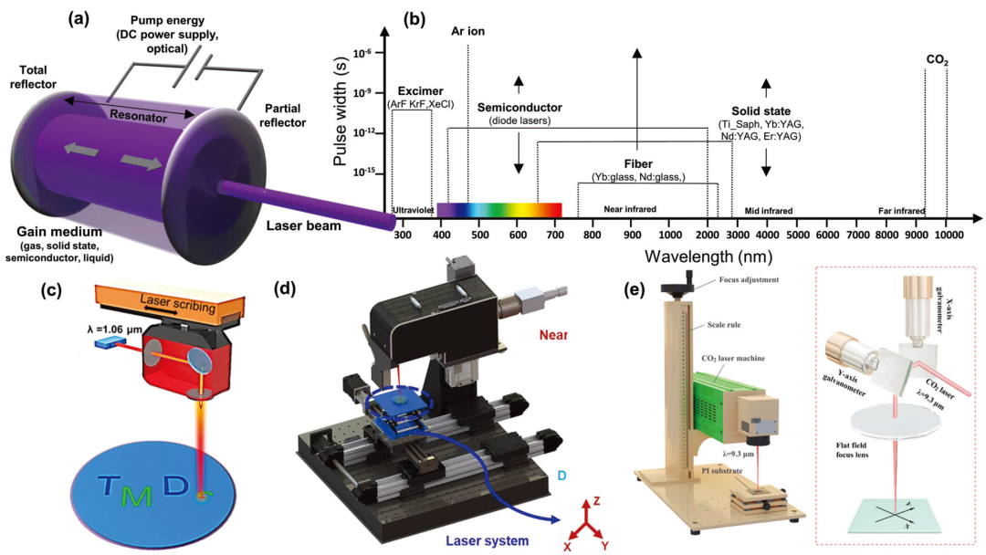
Sources include CO₂ and excimer gas lasers, dye lasers, fiber and other solid-state lasers, and semiconductor diode lasers. Wavelengths span ultraviolet to far infrared, and operation may be continuous or pulsed from milliseconds to femtoseconds.
Three motion architectures are common:
- Moving optics: the objective moves and requires dynamic focus compensation.
- Moving stage: high-precision air-bearing stages provide accuracy but are sensitive to environment and workpiece inertia.
- Galvanometer scanning: mirrors steer the beam rapidly through an f-theta lens; this is usually favored for throughput.
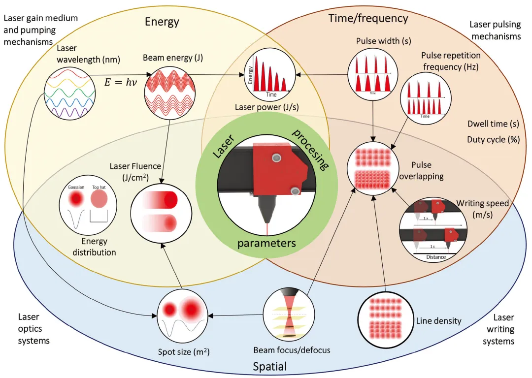
Six parameter groups
1. Wavelength
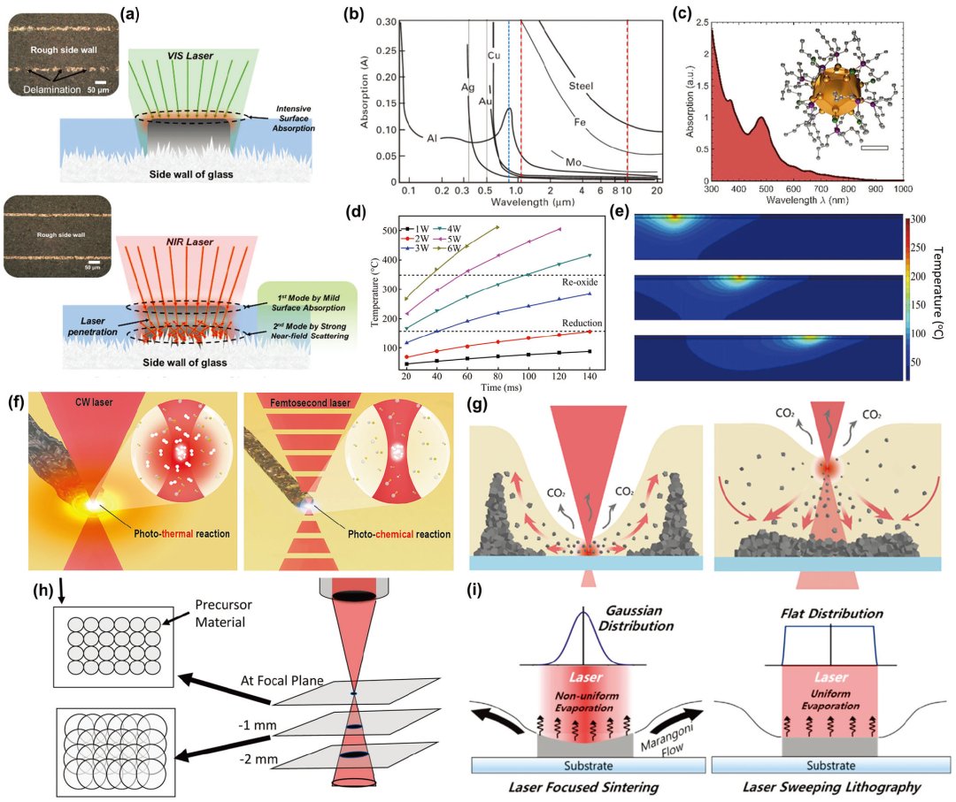
Wavelength selects the interaction mechanism. UV photons more readily trigger photochemical bond formation, isomerization, or breaking and can directly excite semiconductor carriers. Infrared radiation couples strongly to lattice vibration and photothermal conversion. Optical penetration is related to wavelength and extinction coefficient, often written approximately as δ = λ / 4πke; shorter wavelengths usually act nearer the surface, while longer wavelengths may penetrate more deeply.
2. Power
Low power favors photochemistry; intermediate power drives phase or microstructure conversion; higher power sinters and anneals metals and oxides or induces carbonization and graphitization. Excessive power vaporizes or ablates material unintentionally.
3. Writing speed
Power and speed jointly determine local dose. Slow writing raises peak temperature and surrounding heat accumulation; faster writing confines the reaction but may leave incomplete conversion.
4. Pulse width and repetition rate
Long pulses spread heat and favor thermal processes. Femtosecond pulses reach high peak intensity and nonlinear photochemistry with limited diffusion. Repetition rate and speed set pulse overlap, heat accumulation, and conversion efficiency.
5. Focusing and spot size
The optical system and wavelength determine the spot. Focus position can change deposited geometry, while Gaussian and flat-top profiles produce different uniformity and threshold behavior.
6. Processing atmosphere
Argon or nitrogen suppress oxidation and maintain a reducing environment; ambient processing lowers cost but changes material properties; reactive gases can promote a desired reaction or moderate heat accumulation.
Material synthesis and conversion mechanisms
Laser sintering
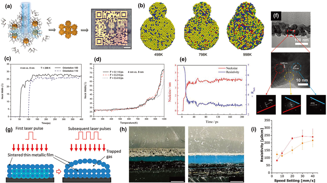
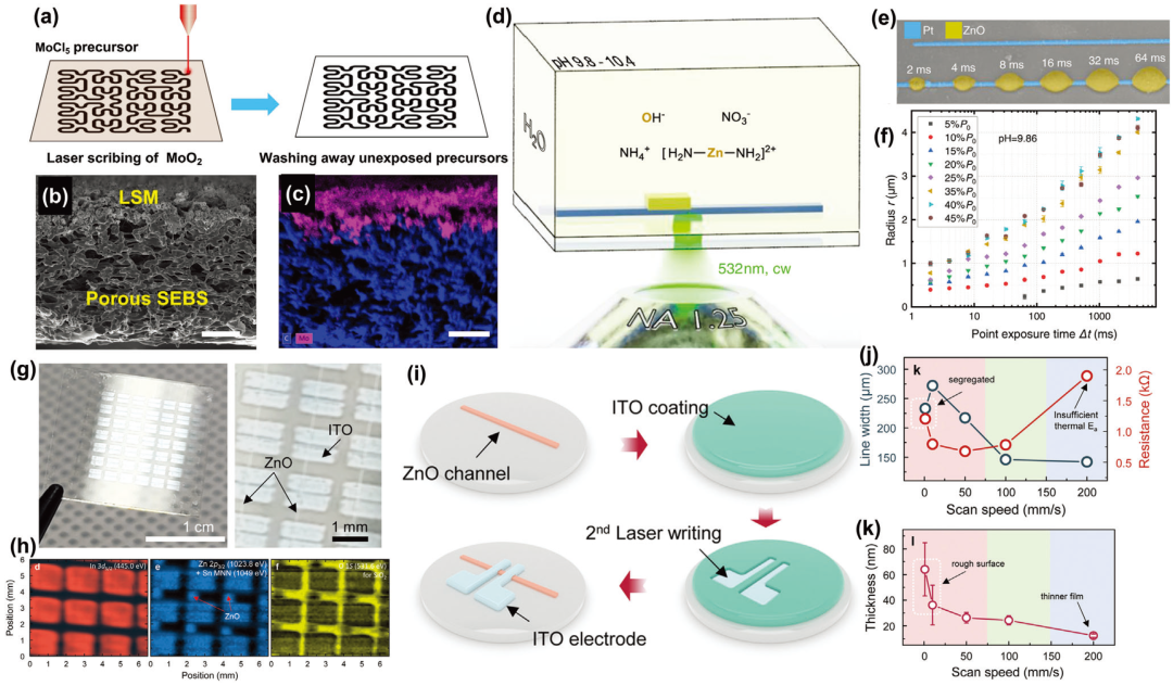
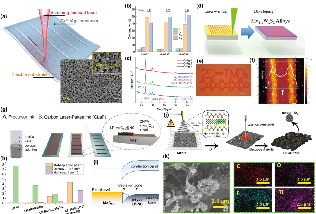
Laser sintering heats nanoparticle films so adjacent particles form and grow necks, reducing surface energy and eventually producing a continuous conductive path. Ultrashort pulses control necking and recrystallization precisely, while selective heating protects glass, silicon, polyimide, PET, and paper substrates. Film thickness must match the thermal and vapor-escape window; thick precursor layers may bubble and become nonuniform.
Laser-induced reduction
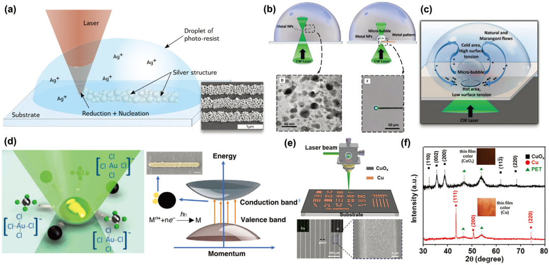
Photons can reduce metal ions to metallic nanoparticles. Multiphoton or two-photon reduction uses high-flux ultrashort pulses; photothermal reduction uses longer pulses or continuous heating to activate a reductant; metal-oxide reduction removes oxygen from CuO, NiO, and related nanoparticle precursors. These low-temperature routes are valuable for conductors and interconnects on sensitive substrates.
Laser-induced oxidation
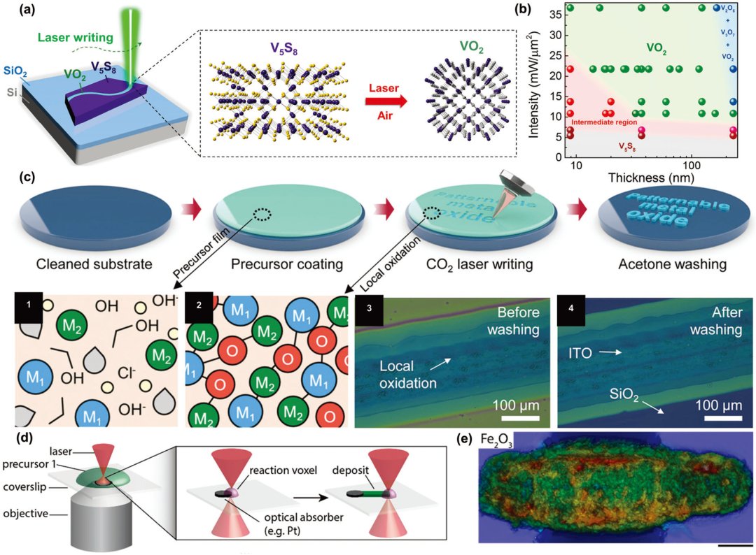
Below the evaporation threshold, irradiation in oxygen can oxidize a metal film through energy absorption, oxygen adsorption and dissociation, nucleation, species transport, and layer growth. The method patterns oxide semiconductors, gate dielectrics, and sensing layers with limited substrate heating.
Laser-induced selective metallization
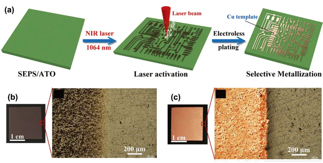
In LISM, a polymer–sensitizer composite is laser activated and then chemically plated. Irradiation decomposes the sensitizer, roughens the surface, and may form catalytic metal nanoparticles. Electroless plating then deposits copper or another metal only on the activated path, enabling conductors and antennas on flexible and three-dimensional substrates.
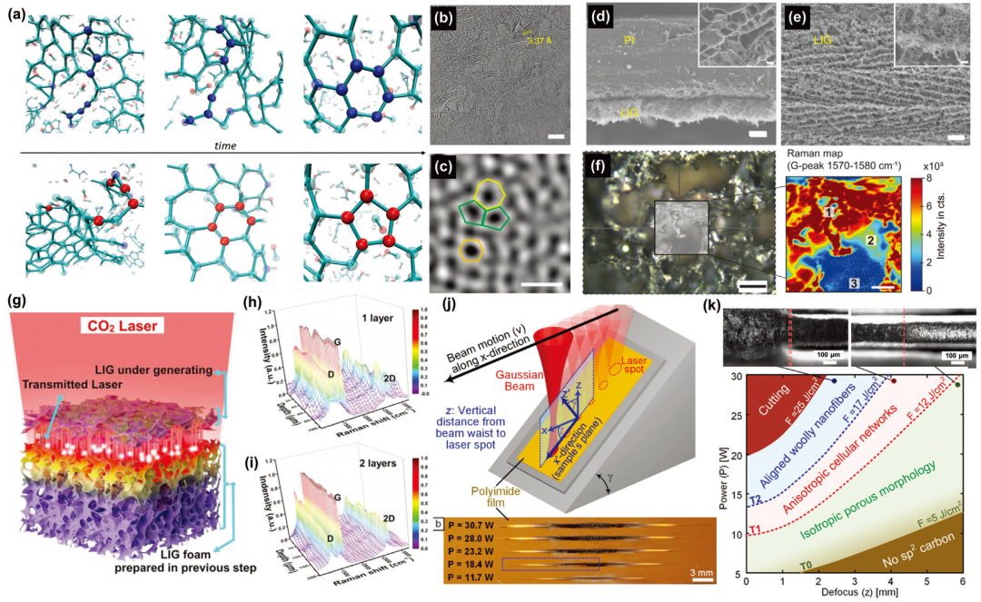
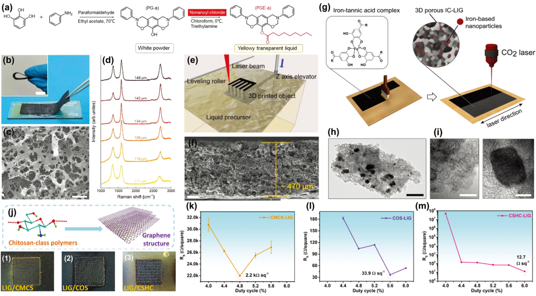
Laser carbonization and graphitization
Photothermal bond breaking removes oxygen-rich volatiles and reorganizes carbon into sp²-rich hexagonal networks. Carbonization produces less ordered carbon; graphitization increases stacked graphitic order.
The Tour group first produced laser-induced graphene (LIG) from polyimide with a CO₂ laser in 2014. LIG is a porous conductive 3D network whose morphology can be tuned from pores to fibers by focus, fluence, and pulse conditions. It is widely studied for electrodes, sensors, and supercapacitors on flexible substrates.
Emerging laser-processed electronic materials
Metal oxides
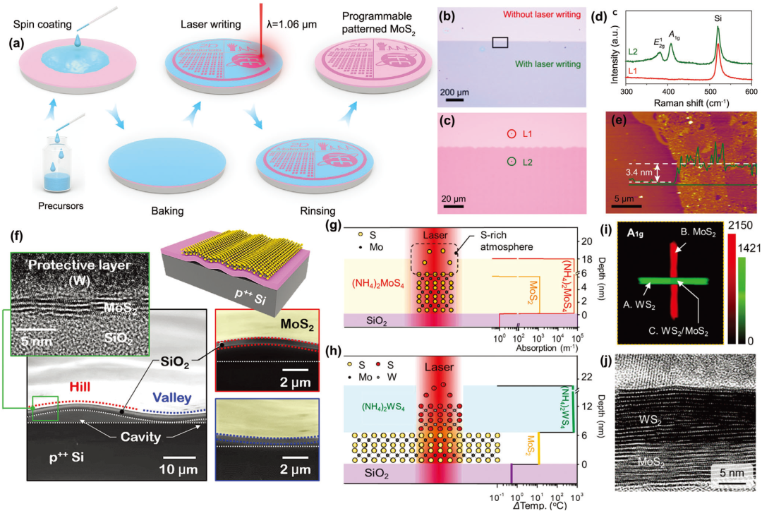
Transition-metal dichalcogenides
Carbides
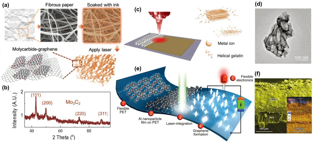
Laser-induced graphene
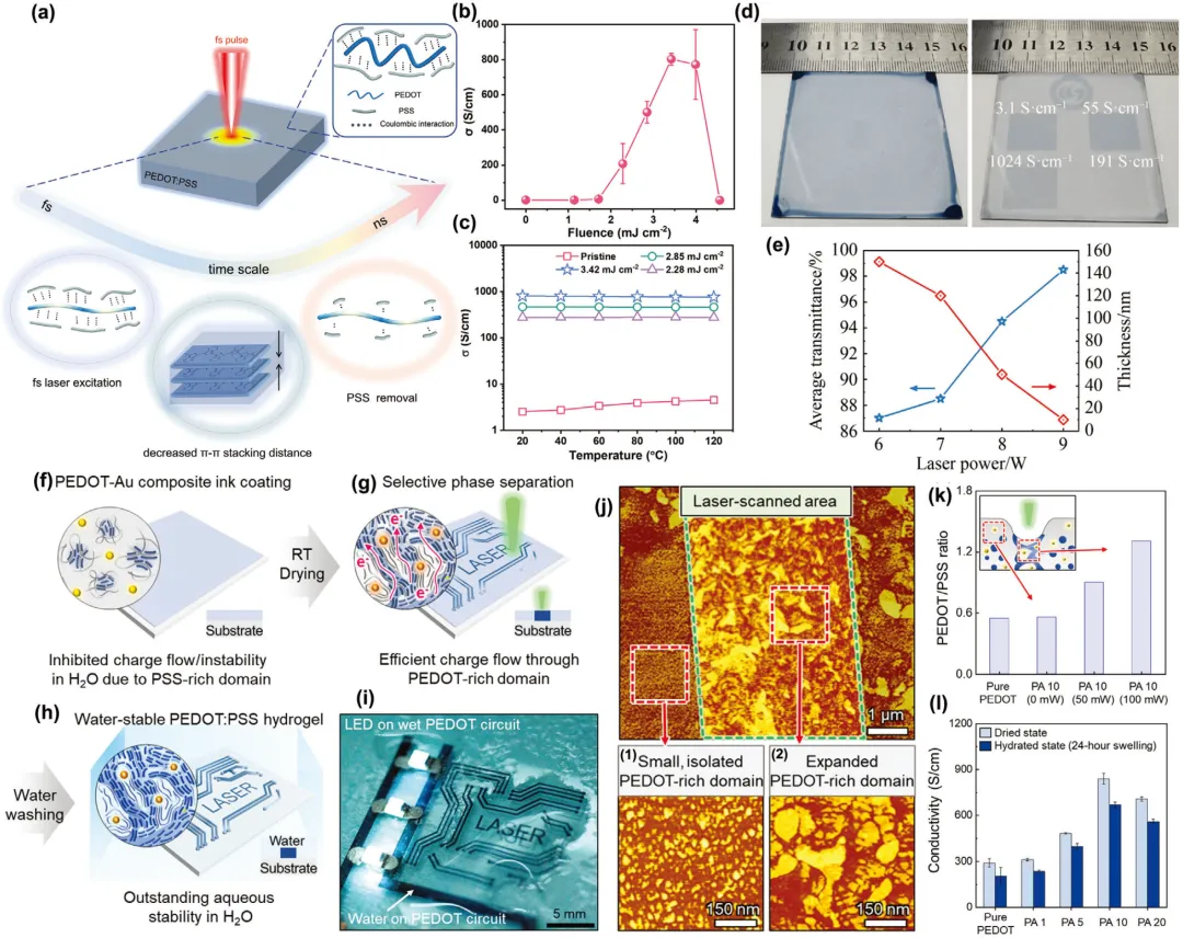
Conductive polymers
Alloys, hybrids, and composites
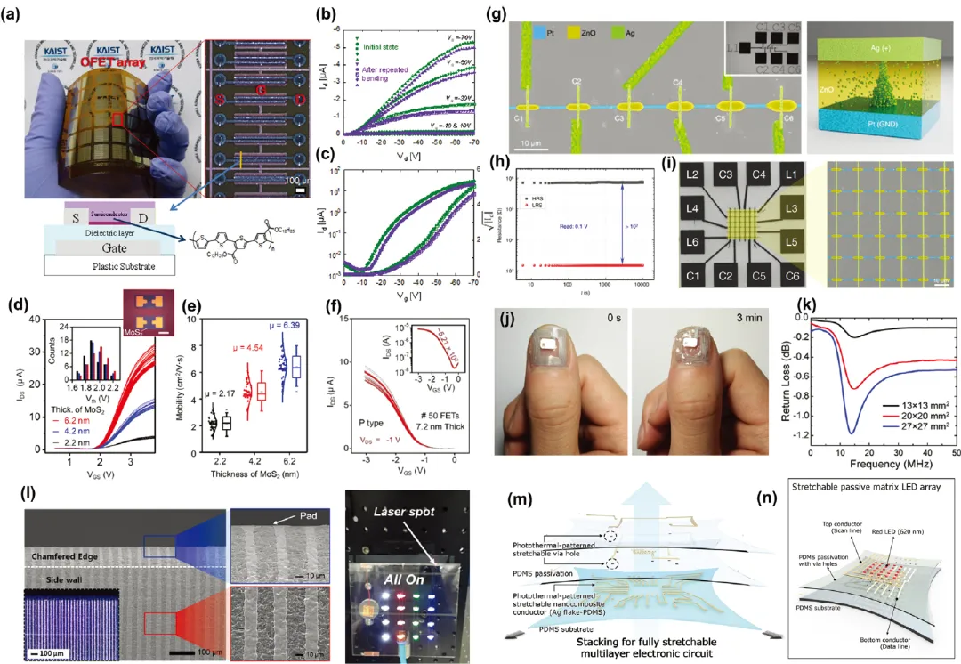
Electronic-device applications
Thin-film transistors, memristors, and interconnects
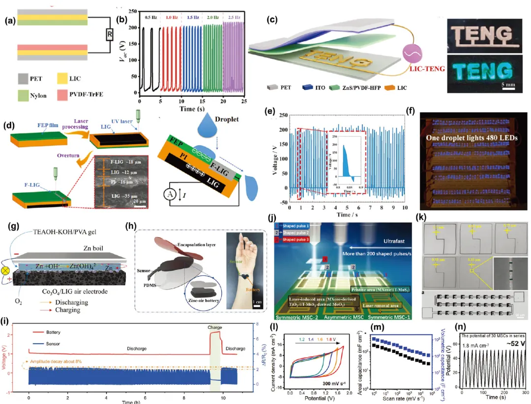
DLW supports flexible organic transistors, MoS₂ and WS₂ FETs, crossbar memristors, physically unclonable security circuits, disposable NFC tags, sidewall interconnects, vias, and stretchable multilayer circuits.
Energy harvesting and storage
Triboelectric nanogenerators, batteries, and microsupercapacitors use laser-written conductors and porous active materials for compact, flexible power systems.
Sensors
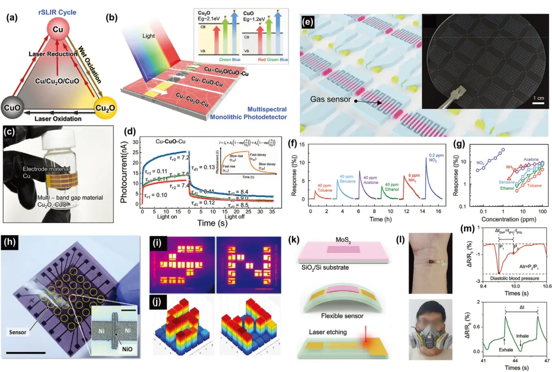
Photodetectors, gas sensors, thermal arrays, and strain sensors benefit from direct patterning, local material conversion, and flexible integration.
Bioelectronic systems
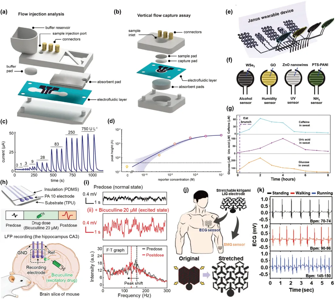
Electrochemical sensors, wearable biochemical monitors, neural interfaces, and conformable electrodes use laser-written flow paths, conductors, and functional surfaces.
Reference
- Pinheiro, Tomás, Morais M., Silvestre S., et al. “Direct Laser Writing: From Materials Synthesis and Conversion to Electronic Device Processing.” Advanced Materials 36.26 (2024). DOI: 10.1002/adma.202402014.
The original Chinese edition was published by “Laser Insights” in Chongqing on March 14, 2025. View the original post. This page preserves the technical body, parameters, figures, conclusions, and reference in a long-form web layout.